
Solar cell and process of manufacturing the same

a solar cell and process technology, applied in the field of solar cell and process of manufacturing the same, can solve the problems of inapplicability to most solar grade materials, which generally have short diffusion lengths, and the cost of photolithography is high, difficult to implement into industrial solar cell production, and disadvantages of photolithography also apply

Inactive Publication Date: 2002-05-07
INTERUNIVERSITAIR MICRO ELECTRONICS CENT (IMEC VZW)
View PDF6 Cites 184 Cited by
  • Summary
  • Abstract
  • Description
  • Claims
  • Application Information

AI Technical Summary

Problems solved by technology

For this concept, high quality material with minority carrier diffusion lengths longer than the cell thickness is needed, which makes this solution not applicable for most solar grade materials which generally have short diffusion lengths.
Photolithography, however, is an expensive processing step and difficult to implement into industrial solar cells production.
The disadvantages of photolithography also apply to this method.
This layer is difficult to combine with industrial metallization techniques such as screen printing metal paste and firing the metal paste which dissolves dielectric layers.
Although this latter case offers also some simplifications to cell processing compared to the ones suggested hereabove, there are still some common drawbacks of cell structures which make use of a large number of holes for electrically connecting the two surfaces of a cell.
Other difficulties arise from the metallization point of view.
The large number of holes associated with the structures disclosed in the patents listed above makes these cell structures expensive and not well suited for mass production.
U.S. Pat. No. 3,903,428 also does not allow a second collecting junction to be placed on the back surface of the cells which would be possible with some of the structures discussed above.
The diffusion of the minority carriers through the whole wafer makes this approach difficult to use for lower quality materials.
The distance a minority carrier can diffuse through the bulk region before it recombines is limited by the material quality.

Method used


Image

  • Solar cell and process of manufacturing the same
  • Solar cell and process of manufacturing the same
  • Solar cell and process of manufacturing the same

Examples


Embodiment Construction

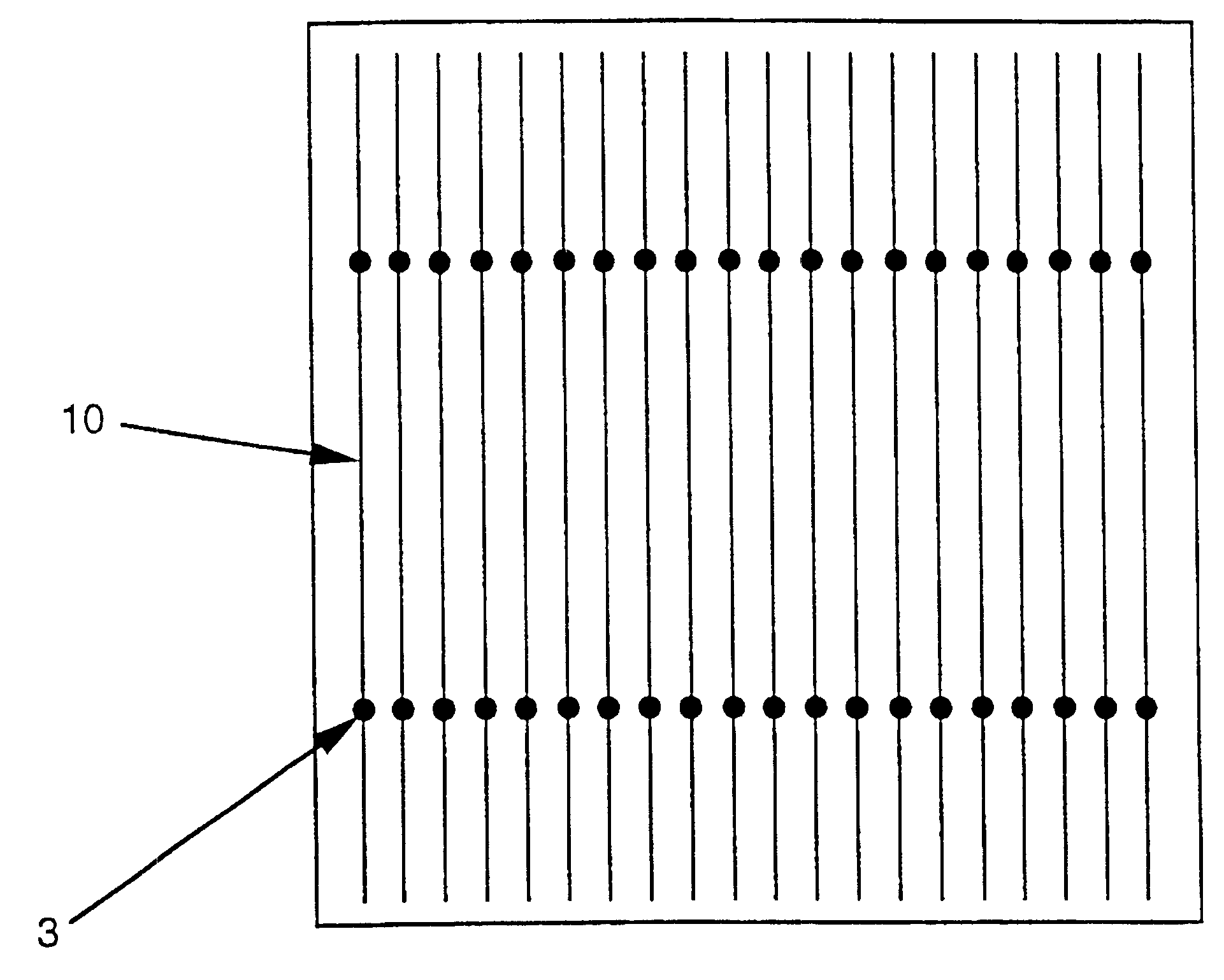
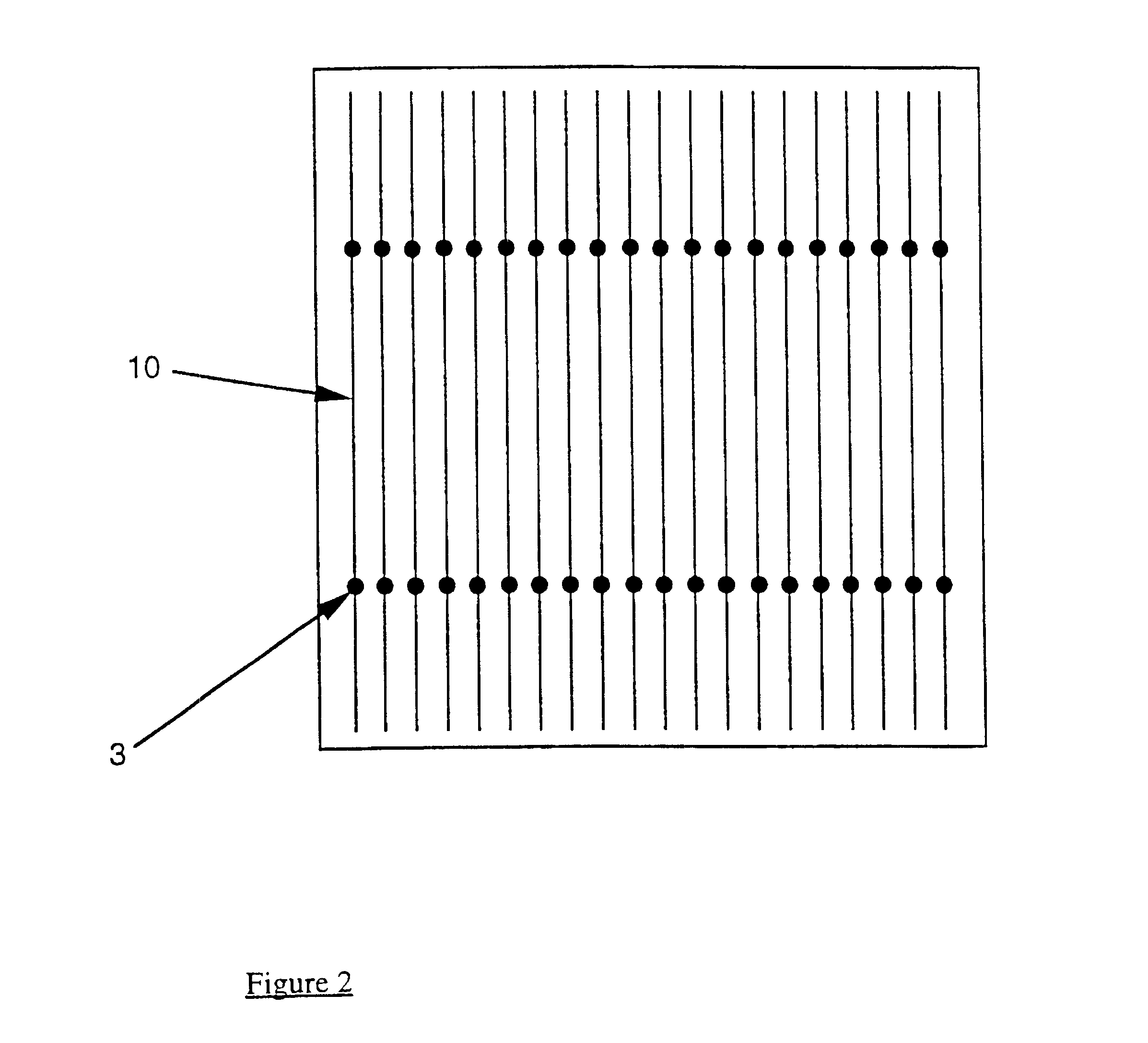
The present solar cell can be described as a parallel connection of two diodes, forming a back contacted double junction solar cell. The current collected by metal fingers at the front surface of the cell is lead to an external contact at its back surface through a limited number of vias. A junction present at the back surface will increase the collection volume of generated carriers, thus increasing the output current of the device.

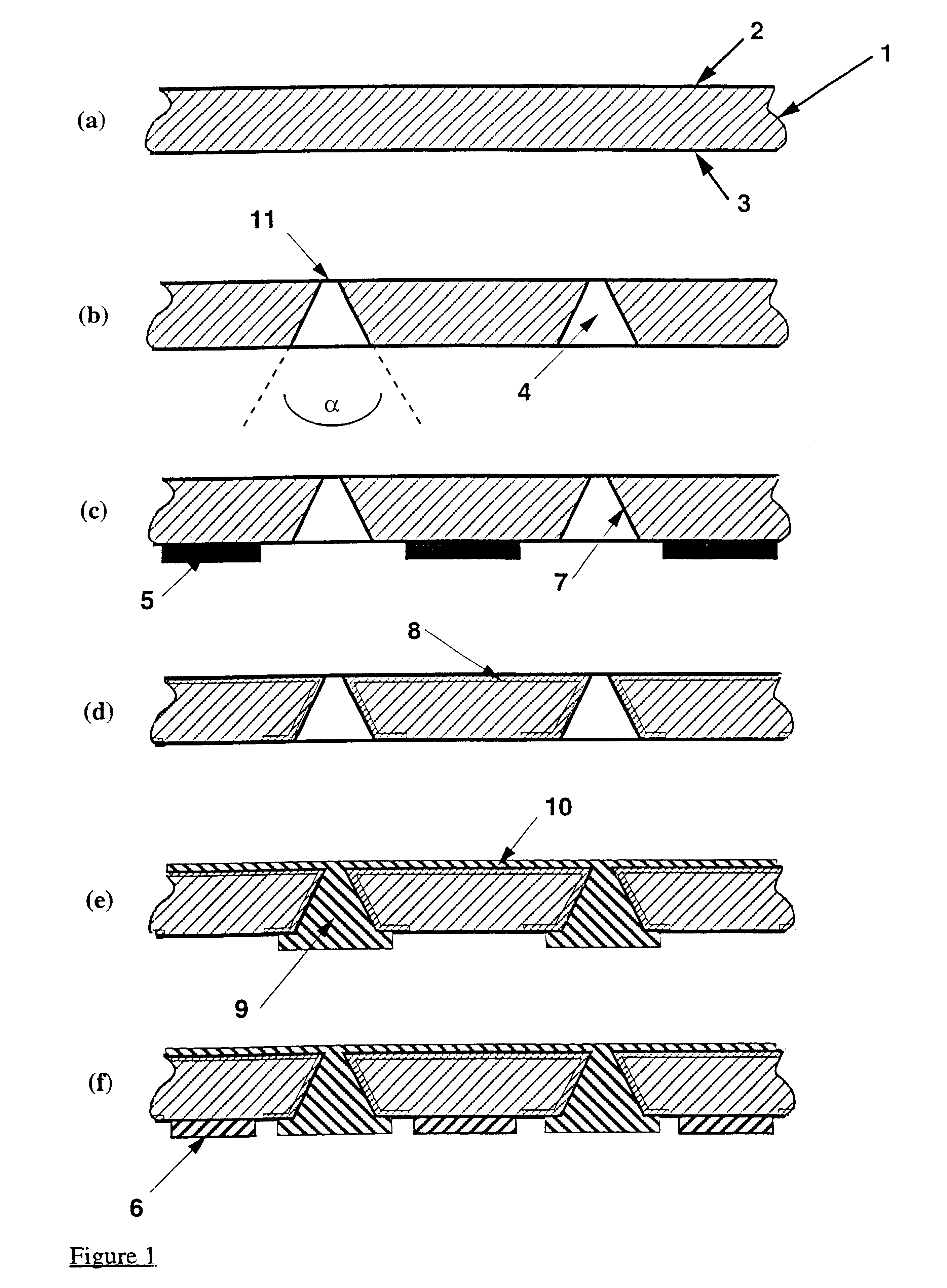
In the following description, a method to produce solar cells with homogeneous emitters is disclosed with reference to FIG. 1.

The processing sequence for a back-contacted solar cell with a double junction is according to a preferred embodiment as follows:

The starting material is a p-type substrate 1 having a front surface 2 and a back surface 3 as represented on FIG. 1a.

On FIG. 1b, a number of vias 4 are machined through the substrate. By using a suitable technique, the opening angles .alpha. of the vias can be varied. Possible techniques for machining h...


PUM


Abstract

The solar cell in the semiconductor substrate includes at least a radiation receiving front surface and a second surface. The substrate includes a first region of one type of conductivity and a second region of the opposite conductivity type with at least a first part located adjacent to the front surface and a second part located adjacent to the second surface. The front surface includes conductive contacts to the second region and the second surface has separated contacts to the first region and to the second region. The contacts to the second region at the second surface are connected to the contacts at the front surface through a limited number of vias.

Description

The present invention is related to solar cells.The present invention is also related to a cost-effective process of realization of solar cells.TECHNOLOGICAL BACKGROUNDMost solar cells described in the prior art can be subdivided into several categories according to their general structure.One of these categories is the group of the so-called back-contacted solar cells, meaning that both ohmic contacts to the two oppositely doped regions of the solar cells are placed on the back or non-illuminated surface of the solar cell. This concept avoids shadowing losses caused by the front metal contact grid on standard solar cells.The most straightforward way to fabricate back contact solar cells is to place the carrier collecting junction between semiconductor regions of opposite doping close to the back surface of the cell ("back-junction" cell). The document "27.5-Percent Silicon Concentrator Solar Cells" (R. A. Sinton, Y. Kwark, J. Y. Gan, R. M. Swanson, IEEE Electron Device Letters, Vol...

Claims


Application Information

Patent Timeline
Patent Type & Authority Patents(United States)
IPC IPC(8): H01L31/0224H01L31/0352H01L31/0248H01L31/18H01L31/04
CPCH01L31/03529H01L31/02245H01L31/1804Y02E10/547Y02P70/50
Inventor KERSCHAVER, EMMANUEL VANSZLUFCIK, JOZEFEINHAUS, ROLANDNIJS, JOHAN
Owner INTERUNIVERSITAIR MICRO ELECTRONICS CENT (IMEC VZW)
Features
  • Generate Ideas
  • Intellectual Property
  • Life Sciences
  • Materials
  • Tech Scout
  • Unparalleled Data Quality
  • Higher Quality Content
  • 60% Fewer Hallucinations
Learn More