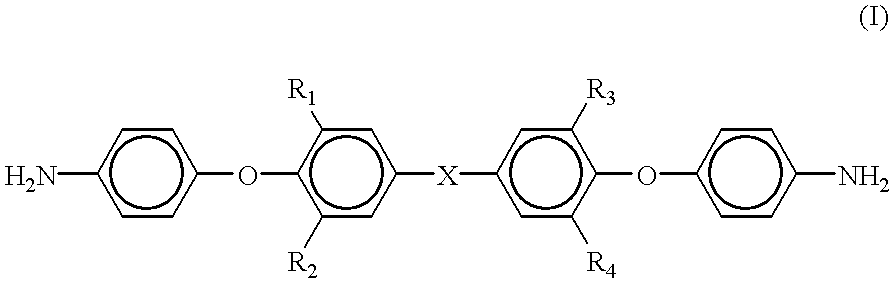
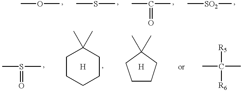
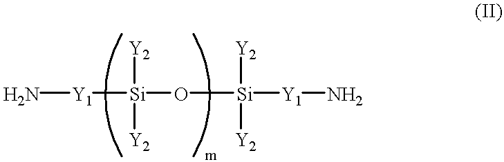
Paste composition, and protective film and semiconductor device both obtained with the same
a technology of protective film and semiconductor device, applied in the direction of polyamide coating, coating, basic electric elements, etc., can solve the problems of cracks running from the inside of the package toward the outside, water absorbed in the package during storage evaporates and expands, and further troubles may arise, so as to achieve good reflow resistance and moisture resistance reliability
- Summary
- Abstract
- Description
- Claims
- Application Information
AI Technical Summary
Benefits of technology
Problems solved by technology
Method used
Image

Examples
example 1
A varnish was prepared by dissolving 128 parts by weight of a polyamide-silicone copolymer (trade name: HIMAL, produced by Hitachi Chemical Co., Ltd.) and 32 parts by weight of an alicyclic epoxy resin (trade name: EHPE 3150, produced by Daicel Chemical Industries, Ltd.) in 250 parts by weight of diethyleneglycol dimethyl ether. Thereto was added 970 parts by weight of a spherical silicon dioxide powder of 30 .mu.m average particle diameter (trade name: FB-74, produced by Denki Kagaku Kogyo K.K.), and then added were 100 parts by weight of a powder of an elastic silicone rubber of 15 .mu.m average particle diameter (trade name: KMP-598, produced by Shin-Etsu Chemical Co., Ltd.), 1 part by weight of a coupling agent (trade name: PRENACT AL-M, produced by Ajinomoto Co, Inc.) and 8 parts by weight of an epoxy curing agent (trade name: AMICURE MY-H, produced by Ajinomoto Co., Inc.), and kneading with three rolls was carried out to prepare a paste composition.
example 2
A varnish was prepared by dissolving 144 parts by weight of a polyamide-silicone copolymer (trade name: HIMAL, produced by Hitachi Chemical Co., Ltd.) and 36 parts by weight of an alicyclic epoxy resin (trade name: EHPE 3150, produced by Daicel Chemical Industries, Ltd.) in 250 parts by weight of diethyleneglycol dimethyl ether. Thereto was added 970 parts by weight of a spherical silicon dioxide powder of 30 .mu.m average particle diameter (trade name: FB-74, produced by Denki Kagaku Kogyo K.K.), and then added were 100 parts by weight of a powder of an elastic silicone rubber of 15 .mu.m average particle diameter (trade name: KMP-598, produced by Shin-Etsu Chemical Co., Ltd.), 1 part by weight of a coupling agent (trade name: PRENACT AL-M, produced by Ajinomoto Co, Inc.) and 8 parts by weight of an epoxy curing agent (trade name: AMICURE MY-H, produced by Ajinomoto Co., Inc.), and kneading with three rolls was carried out to prepare a paste composition.
example 3
On the mounting faces of chip-supporting boards 5 mounted as described above with semiconductor elements 2 were potted 0.8 g portions of the paste composition A, so that semiconductor elements 2 and gold wires 4 were completely covered. Chip-supporting boards 5 with the potted paste composition were placed in an oven, and heated at 70.degree. C. for one hour, at 120.degree. C. for one hour and at 160.degree. C. for one hour by elevating temperature stepwise, to dry and solidify the paste composition. Thus semiconductor devices packaged with cured sealing materials 1a were obtained.
PUM
| Property | Measurement | Unit |
|---|---|---|
| Temperature | aaaaa | aaaaa |
| Time | aaaaa | aaaaa |
| Time | aaaaa | aaaaa |
Abstract
Description
Claims
Application Information
 - R&D Engineer
- R&D Manager
- IP Professional
- Industry Leading Data Capabilities
- Powerful AI technology
- Patent DNA Extraction
Browse by: Latest US Patents, China's latest patents, Technical Efficacy Thesaurus, Application Domain, Technology Topic.
© 2024 PatSnap. All rights reserved.Legal|Privacy policy|Modern Slavery Act Transparency Statement|Sitemap