Vertical trench-formed dual-gate FET device structure and method for creation

a technology of vertical trenches and fets, applied in the field of vertical trenches, can solve the problems of increasing production costs, reducing semiconductor reliability and performance, and limiting the fet scaling by the formation and control of such gates

Inactive Publication Date: 2002-06-18
IBM CORP
View PDF12 Cites 137 Cited by
  • Summary
  • Abstract
  • Description
  • Claims
  • Application Information

AI Technical Summary

Problems solved by technology

However, as gate lengths are formed below 50 nm, FET scaling becomes limited by the formation and control of such gates.
Furthermore, the smaller FETs may require a larger number of contacts on a single chip.
The limitations of controlling gates scaled below 50 nm, as well as the requirement of a plurality of contacts on a single FET, produce a variety of problems such as alignment problems, problems associated with making connections with contacts, gate length control, and low FET resistance, for example.
Overall, the above problems have the effect of decreasing semiconductor reliability and performance, as well as leading to increased production costs.
However, the known techniques of forming FETs having vertical gates and increased surface space are not sufficient in forming and controlling smaller gate electrodes, such as those scaled below 50 nm, as well as increased surface space as a result of such smaller gates.
Forming and controlling smaller gates by known techniques leads to semiconductors having decreased performance and reliability.

Method used


Image

  • Vertical trench-formed dual-gate FET device structure and method for creation
  • Vertical trench-formed dual-gate FET device structure and method for creation
  • Vertical trench-formed dual-gate FET device structure and method for creation

Examples


Embodiment Construction

)

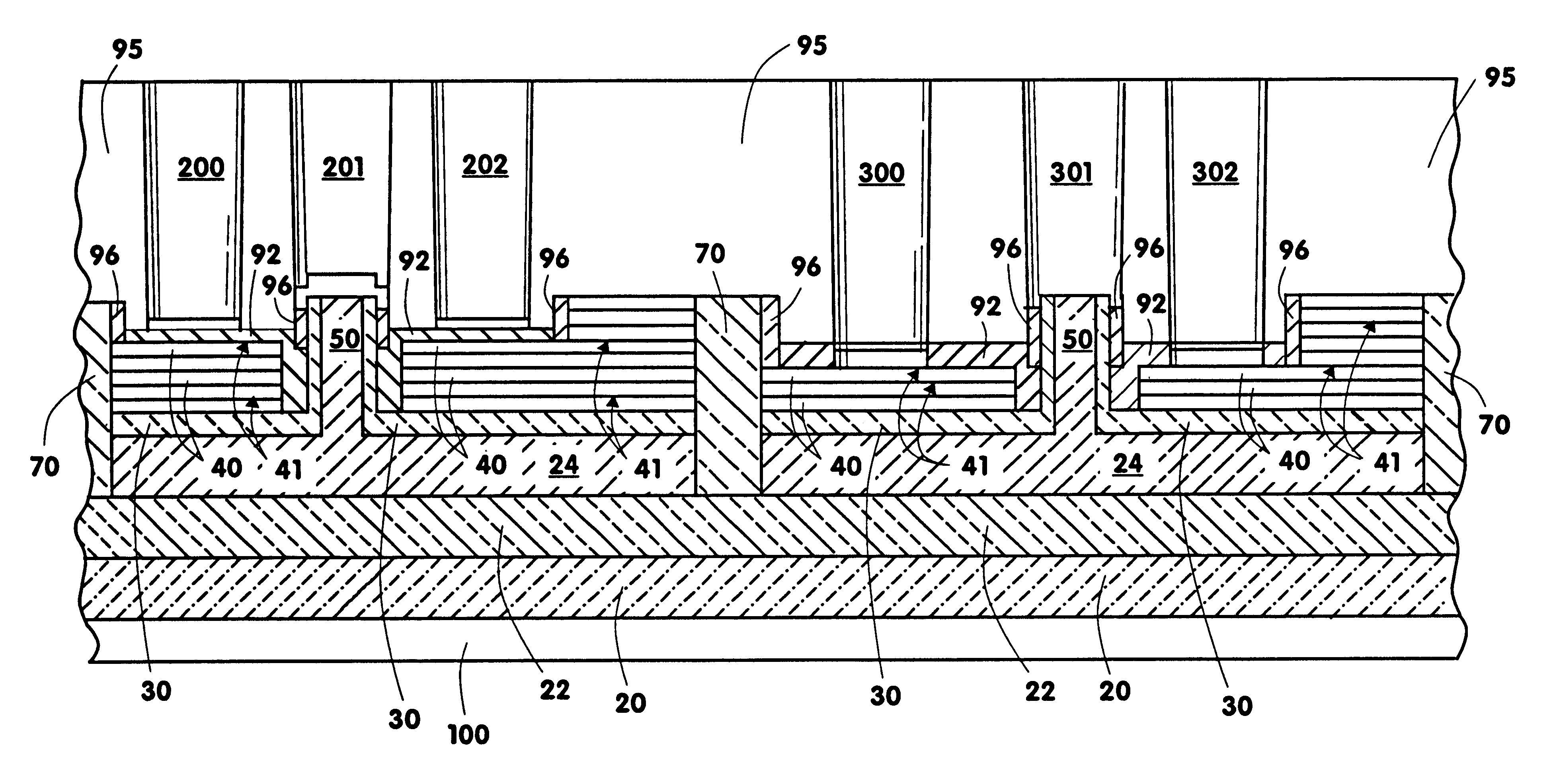
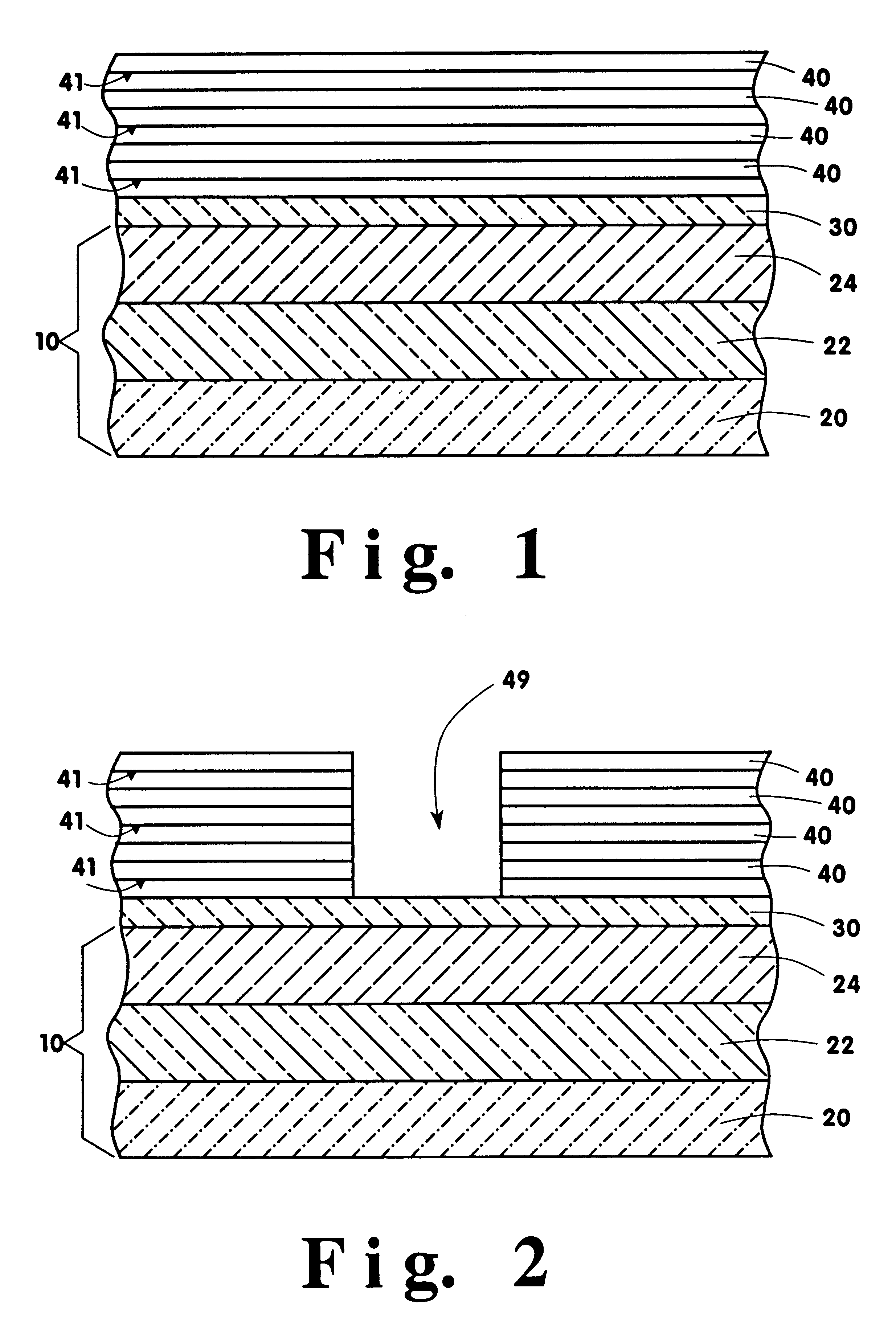
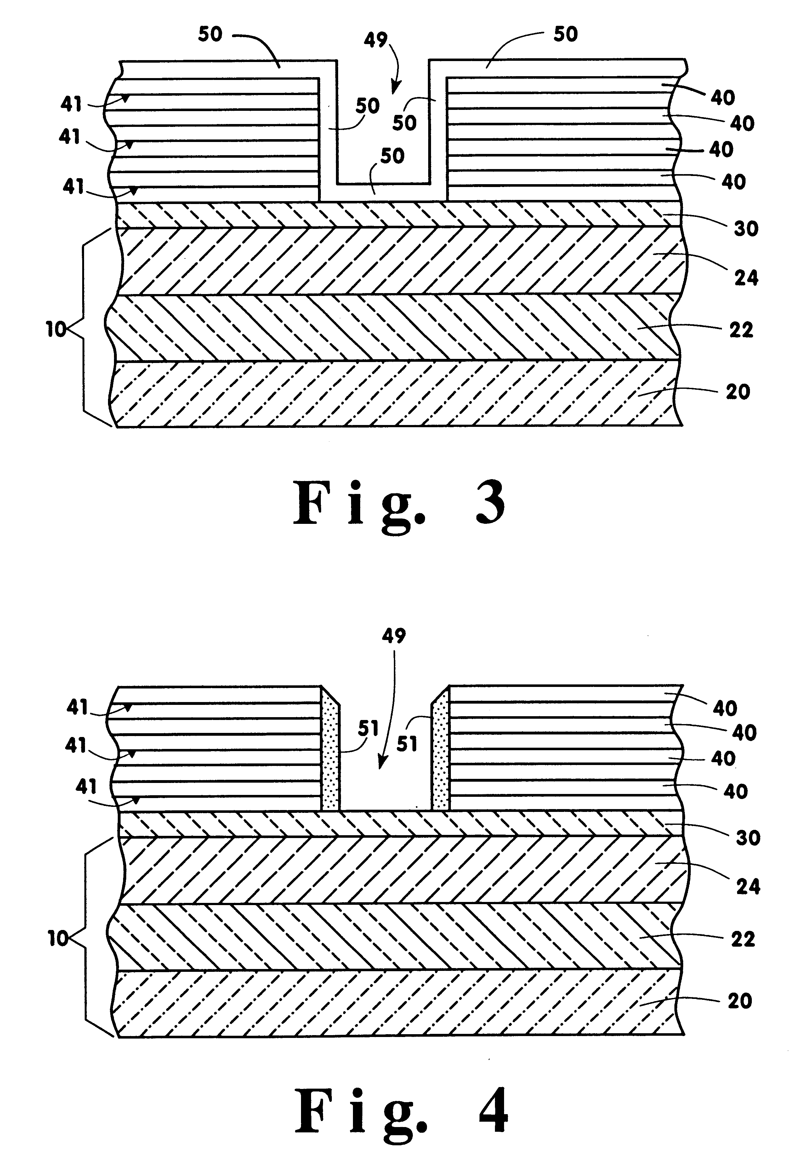
In describing the preferred embodiment of the present invention, reference will be made herein to FIGS. 1-15 of the drawings in which like numerals refer to like features of the invention. Features of the invention are not necessarily shown to scale in the drawings.

FIGS. 1-15 show a preferred embodiment of the present invention comprising a FET, and a method of making the same, having a vertical trench formed double-gate with a plurality of nitride layers having oxide marker etch stop layers provided periodically there-through. The present invention provides for control and formation of gate lengths scaled down to about 5 nm to about 100 nm, more preferably from about 5 nm to about 50 nm. The plurality of nitride layers in combination with the oxide marker layers enable the fabrication of a plurality of vertical channel FETs with varying gate lengths on a single die. In doing so, the plurality of nitride layers and oxide etch stop layers allow a FET to be fabricated with any of a v...


PUM

PropertyMeasurementUnit
thicknessaaaaaaaaaa
gate lengthsaaaaaaaaaa
lengthsaaaaaaaaaa

Abstract

The present invention relates to an apparatus and method of forming one or more FETs having a vertical trench-formed double-gate, with a plurality of nitride layers having oxide marker etch-stop layers provided periodically there-through, thereby adapting the FETs to have a plurality of selectable gate lengths. The present invention provides for control and formation of gate lengths scaled down to about 5 nm to about 100 nm, preferably from about 5 nm to about 50 nm. The plurality of pad nitride layers with the oxide etch-stop layers provide for the present FET to be connected to a plurality of contacts having a variety of connection depths corresponding to the gate lengths used, by etching a plurality of via in the pad nitride layers whereby such vias stop at selected ones of the etch-stop layers to provide vias adapted to connect with the selected ones of such contacts. Additional gate material may be deposited over a top surface of the selected plurality of nitride layers to allow for contacts to the gate electrodes of any given FET.

Description

1. Field of the InventionThe present invention relates generally to field-effect transistors (FET). More particularly, the present invention relates to an apparatus and method for forming a vertical double-gated FET having a pad nitride layer with a plurality of etch stop layers periodically there-through which provide the ability to fabricate a plurality of vertical-channel FETs with a variety of gate lengths on the same die.2. Description of Related ArtOver the years, it has been indispensably necessary to reduce semiconductor device size in order to increase performance and decrease power consumption. As a result of such smaller semiconductors, an increased number of smaller integrated circuit contacts are required for making connections to such semiconductors.In keeping up with modern technology, integrated circuits, such as field effect transistors (FETs), may be formed with gate lengths scaled below 50 nm. However, as gate lengths are formed below 50 nm, FET scaling becomes li...

Claims


Application Information

Patent Timeline
Patent Type & Authority Patents(United States)
IPC IPC(8): H01L29/786H01L29/40H01L21/70H01L21/84H01L29/66H01L29/423H01L27/12
CPCH01L21/84H01L27/1203H01L29/78648H01L29/78642H01L29/42384
Inventor AGNELLO, PAUL D.BALLANTINE, ARNE W.DIVAKARUNI, RAMACHANDRAJONES, ERIN C.NOWAK, EDWARD J.RANKIN, JED H.
Owner IBM CORP
Why Eureka
Try Eureka