Laterally diffused metal-oxide-semiconductor device and method of making the same

a metal-oxide-semiconductor and lateral diffusion technology, applied in the direction of semiconductor devices, basic electric elements, electrical appliances, etc., can solve the problems of undetectable affecting the performance and reliability of the device, the localized and non-uniform buildup of interface states and oxide charges near and underneath, and the device to burn out in advance. , to achieve the effect of reducing the impact of hot carrier and increasing the idlin

Active Publication Date: 2009-03-19
UNITED MICROELECTRONICS CORP
View PDF5 Cites 79 Cited by
  • Summary
  • Abstract
  • Description
  • Claims
  • Application Information

AI Technical Summary

Benefits of technology

[0012]An objective of the present invention is to provide a laterally diffused metal-oxide-semiconductor (LDMOS) device and a method of making the LDMOS device. In the LDMOS of the present invention, hot carrier impact is minimized and Idlin is increased.

Problems solved by technology

1. In order to lower Vt (threshold voltage) of LDMOS or increase Idlin (linear drive current), a thin gate dielectric layer is preferred in the channel region.
2. Following the term 1, a serious hot carrier injection (HCI) issue will occur, leading the device to burn out in advance.
HCl in an MOS device generally results from heating and subsequent injection of carriers into the gate oxide of the device, which results in a localized and non-uniform buildup of interface states and oxide charges near and underneath a gate of the device.
This phenomenon can produce variations in certain characteristics of the MOS device, including threshold voltage, transconductance, drain current, etc., thus undesirably affecting the performance and reliability of the device.
Currently, an increased field oxidation layer (FOX) width or an offset of drain side to the gate is used in order to decrease hot carrier injection issue, thus the device pitch is enlarged and Idlin performance is deteriorated, and finally a high Rdson (drain-source on-state resistance) is caused, and the performance and reliability of the device are undesirably affected.

Method used


Image

  • Laterally diffused metal-oxide-semiconductor device and method of making the same
  • Laterally diffused metal-oxide-semiconductor device and method of making the same
  • Laterally diffused metal-oxide-semiconductor device and method of making the same

Examples


Embodiment Construction

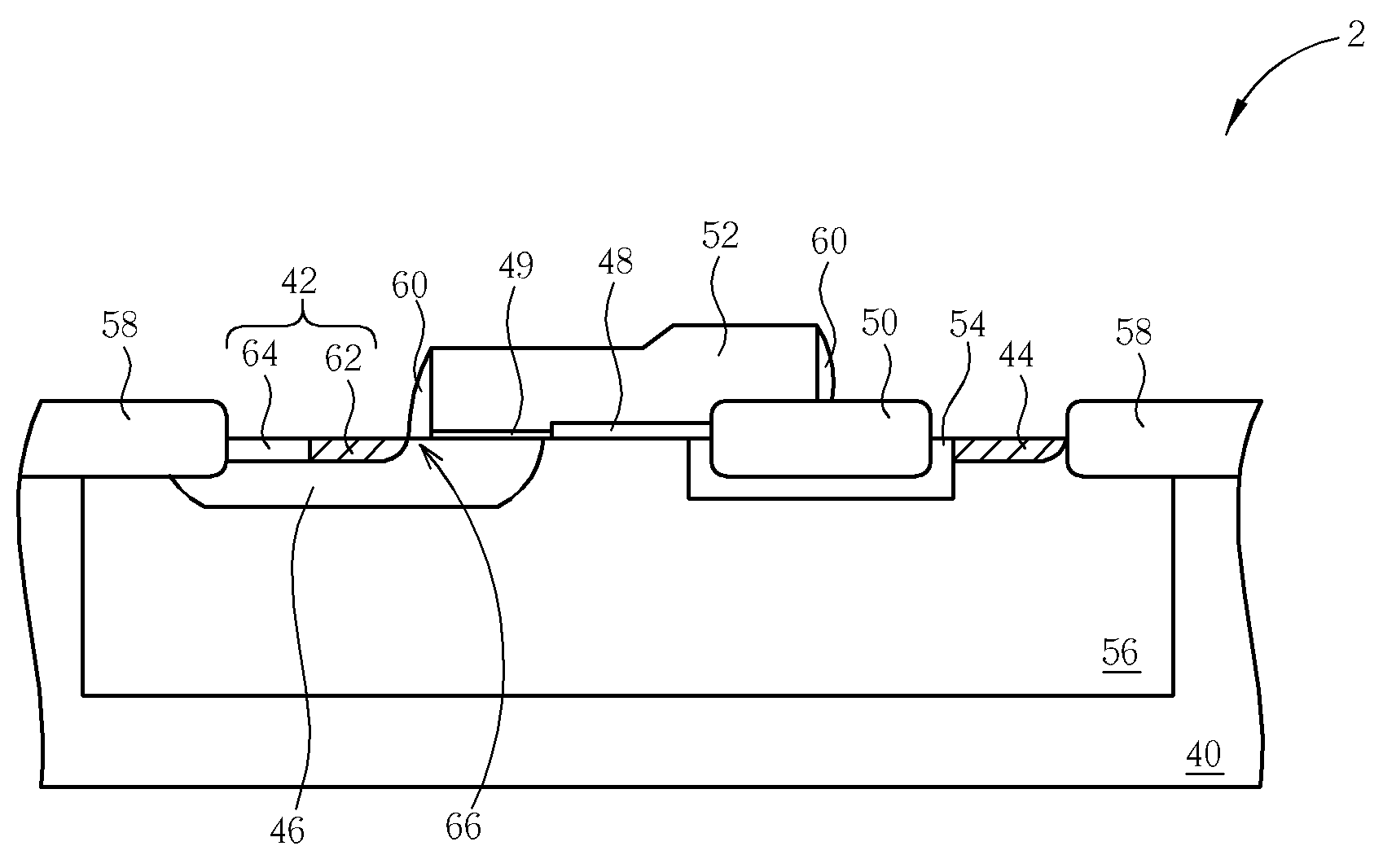
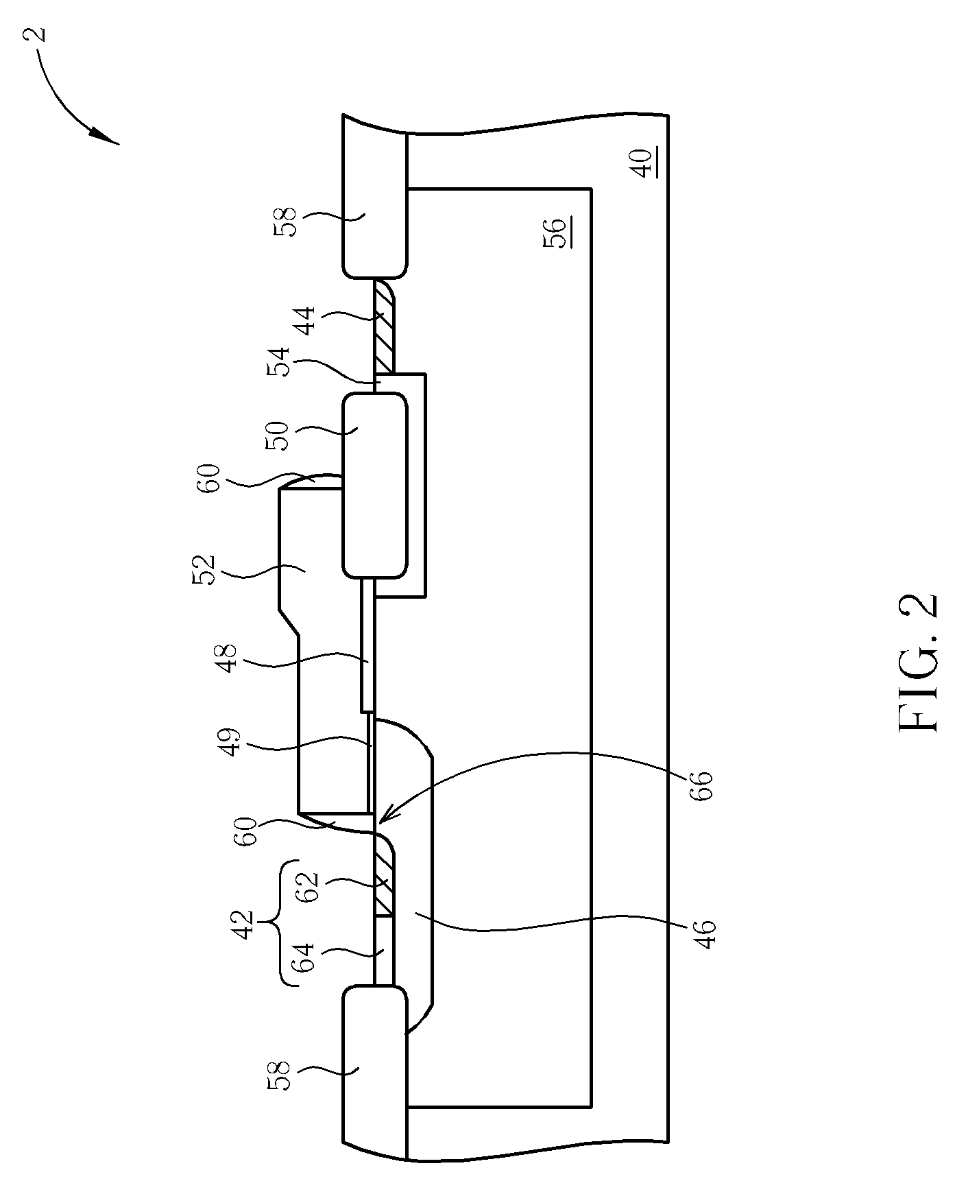
[0020]FIG. 2 is a schematic cross-sectional diagram illustrating the LDNMOS device in accordance with one preferred embodiment of this invention. It is understood that the electric polarities shown in figures are exemplary, and suitable modification of the polarities can be made to form an LDPMOS device.

[0021]According to the preferred embodiment, the LDNMOS device 2 is formed on an active area of a semiconductor substrate 40 such as a P-type silicon substrate and a deep N-well 56 may be formed in the P-type silicon substrate, or a semiconductor substrate such as an N-type silicon substrate may be used. The active area is defined and isolated with a peripheral field oxide layer 58. The LDNMOS device 2 comprises a source region 42, a gate 52 and a drain 44. The source region 42 may further comprise a heavily N-doped source doping region 62 and a heavily P-doped region 64 bordering upon each other, both of which are formed within a P-body 46. The drain 44 may be a heavily N-doped drai...


PUM


Abstract

A laterally diffused metal-oxide-semiconductor (LDMOS) device as well as a method of making the same is disclosed. A gate is formed on a semiconductor substrate between a source region and a drain region with one side laterally extending onto a part of a field oxide layer and the opposite side beside the source region. A gate dielectric layer is formed between the gate and the semiconductor substrate, wherein the gate dielectric layer comprises two or more portions having different thicknesses arranged laterally in a way that the thicknesses of the portions gradually increase from one side beside the source doping region to the opposite side bordering the field oxide layer. With such structure, the hot carrier impact is minimized and the gate length can be scaled down to gain Idlin.

Description

BACKGROUND OF THE INVENTION [0001]1. Field of the Invention[0002]The present invention relates to a laterally diffused metal-oxide-semiconductor (LDMOS) device and, more particularly, to a LDMOS device with a reduced hot carrier injection effect.[0003]2. Description of the Prior Art[0004]Power MOS devices, including laterally diffused metal-oxide-semiconductor (LDMOS) devices, are employed in a variety of applications, such as, for example, power amplifiers in wireless communications systems. Especially, LDMOS device using Vg (gate voltage)=5V seems to become a main stream in the application. The Vd (drain voltage) of such LDMOS may be a various voltage depending on device's application.[0005]FIG. 1 schematically illustrates a cross-sectional view of a conventional laterally diffused NMOS device. The conventional laterally diffused NMOS device 1 is fabricated on an active area of a semiconductor substrate 10 such as a P-type semiconductor substrate. The active area is isolated by a ...

Claims


Application Information

Patent Timeline
Patent Type & Authority Applications(United States)
IPC IPC(8): H01L29/78H01L21/336
CPCH01L29/42368H01L29/7816H01L29/66689H01L29/66681
Inventor CHEN, CHIN-LUNGLI, WEN-KUO
Owner UNITED MICROELECTRONICS CORP
Why Eureka
Try Eureka