Technique to mitigate short channel effects with vertical gate transistor with different gate materials

a technology of vertical gate transistor and short channel effect, which is applied in the direction of semiconductor devices, basic electric elements, electrical appliances, etc., can solve the problems of deviation from the predictable performance of larger scaled devices, difficult to scale junction depths to under 100 nm dimensions, and difficult to produce sub-micron devices that can perform as desired, etc., to achieve small effective channel length, reduce the effect of effective channel length

Inactive Publication Date: 2002-09-19
MICRON TECH INC
View PDF2 Cites 76 Cited by
  • Summary
  • Abstract
  • Description
  • Claims
  • Application Information

AI Technical Summary

Benefits of technology

[0005] This invention relates to a process of forming a transistor having three adjacent gate electrodes and the resulting transistor. In forming such a transistor it is possible to mitigate short channel effects as MOSFET structures are scaled down to sub-micron sizes. This transistor fabrication process can utilize different materials for the gate electrodes so that the workfunctions of the three gate electrodes can be tailored to be different. The three gate electrodes can be connected by a single conducting line and all three are positioned over a single channel and operate as a single gate having a pair of outer gate regions and an inner gate region. This allows for use with higher source and drain voltages. These devices provide for higher performance, using a standard or scaled down transistor surface area, than can be achieved with conventional transistor structure. They have smaller effective channel lengths when "on," and consequently, faster speeds are achievable. The devices have longer channel lengths when "off," thereby mitigating short channel effects.

Problems solved by technology

As the industry standard approaches smaller and smaller scaled devices, problems with further advancement are presented and it becomes more difficult to produce sub-micron devices that can perform as desired.
However, it is extremely difficult to scale junction depths to under 100 nm dimensions because these are doped by ion implantation and thermally activated.
For shorter channel devices (channel lengths below 2 .mu.m) a series of effects arise that result in deviations from the predictable performance of larger scaled devices.
The problem with such structures is that gate oxides are already approaching theoretical minimal values, therefore, regions of even thinner gate oxides pose reliability risks.

Method used


Image

  • Technique to mitigate short channel effects with vertical gate transistor with different gate materials
  • Technique to mitigate short channel effects with vertical gate transistor with different gate materials
  • Technique to mitigate short channel effects with vertical gate transistor with different gate materials

Examples


Embodiment Construction

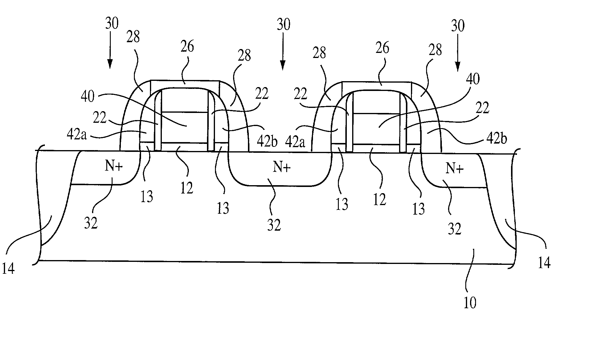
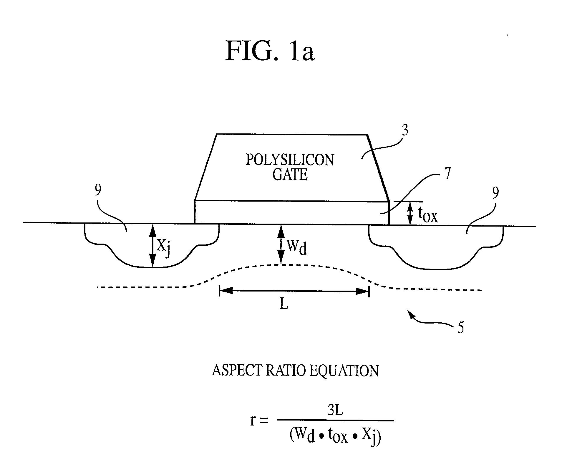
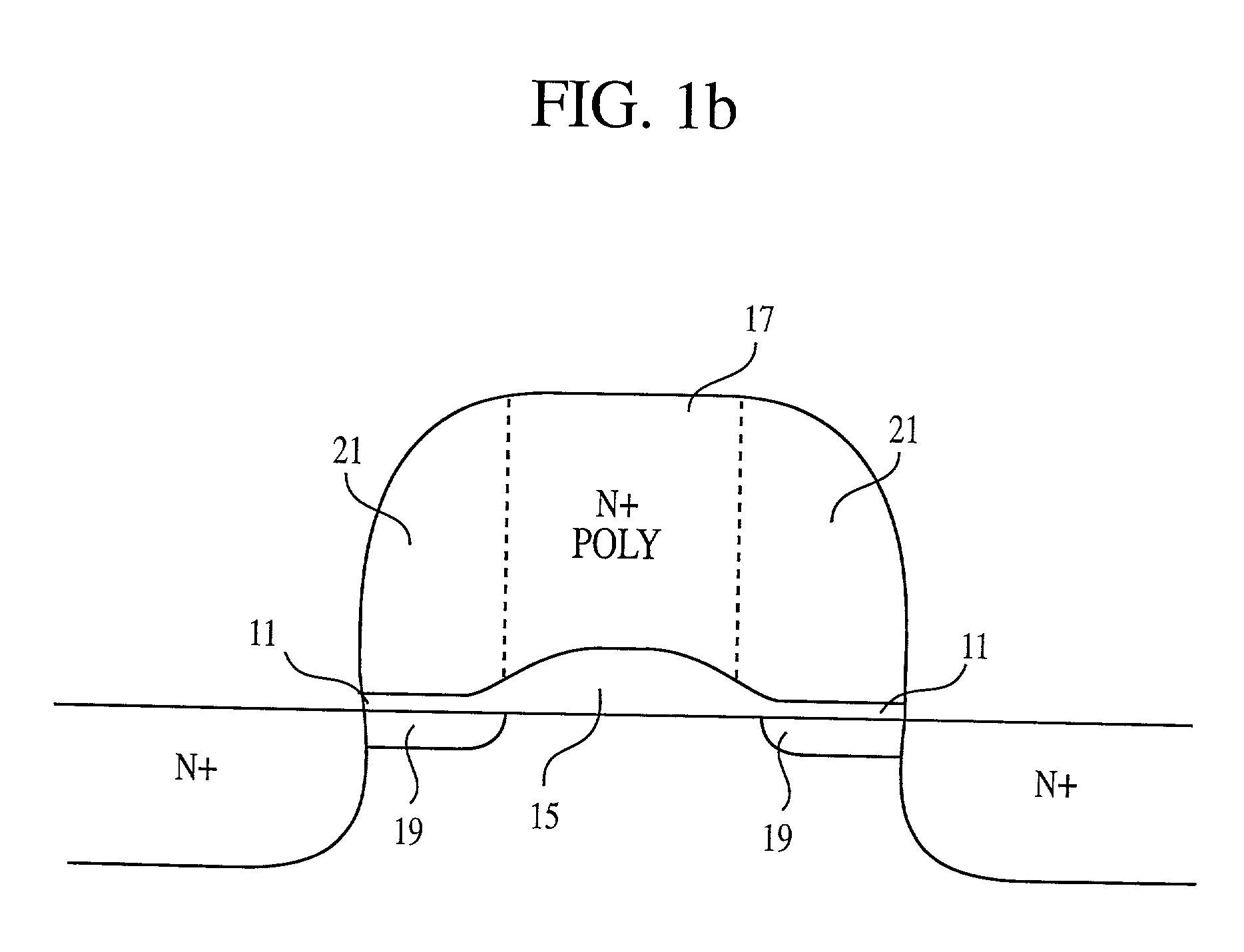
[0016] In the following detailed description, reference is made to various specific embodiments of the invention. These embodiments are described with sufficient detail to enable those skilled in the art to practice the invention, and it is to be understood that other embodiments may be employed, and that structural and electrical changes may be made without departing from the spirit or scope of the present invention.

[0017] In the following discussion the terms "wafer" and "substrate" are used interchangeably and are to be understood to refer to any type of semiconductor substrate, including silicon, silicon-on-insulator (SOI), and silicon-on-sapphire (SOS) technology, and other semiconductor structures. Furthermore, references to a "wafer" or "substrate" in the following description, do not exclude previous processing steps utilized to form regions or junctions in or on the base semiconductor structure or foundation.

[0018] No particular order is required for the method steps descri...


PUM


Abstract

This invention relates to a process of forming a transistor with three vertical gate electrodes and the resulting transistor. By forming such a transistor it is possible to maintain an acceptable aspect ratio as MOSFET structures are scaled down to sub-micron sizes. The transistor gate electrodes can be formed of different materials so that the workfunctions of the three electrodes can be tailored. The three electrodes are positioned over a single channel and operate as a single gate having outer and inner gate regions.

Description

FIELD OF THE INVENTION[0001] This invention relates to the field of semiconductor transistors that are scaled down to sub-micron sizes.BACKGROUND OF THE INVENTION[0002] There is ever-present pressure in the semiconductor industry to develop smaller and more highly integrated devices. As the industry standard approaches smaller and smaller scaled devices, problems with further advancement are presented and it becomes more difficult to produce sub-micron devices that can perform as desired.[0003] As MOSFET are scaled to deep sub-micron dimensions it becomes increasingly difficult to maintain an acceptable aspect ratio, as shown in FIG. 1a. FIG. 1a shows a representational illustration of a MOSFET having a polysilicon gate 3 over a substrate 5, with the two being separated by a gate oxide 7. Source and drain regions 9 of the substrate are on either side of the gate structure, forming a transistor. The aspect ratio equation represents the spatial relationship between the elementary part...

Claims


Application Information

Patent Timeline
Patent Type & Authority Applications(United States)
IPC IPC(8): H01L21/28H01L21/8242H01L29/49H01L29/78
CPCH01L21/28105H01L27/10873H01L29/4983H01L29/7831H10B12/05
Inventor FORBES, LEONARDTRAN, LUAN C.AHN, KIE Y.
Owner MICRON TECH INC
Why Eureka
Try Eureka