Method and system for performing capacitance estimations on an integrated circuit design routed by a global routing tool

a global routing and capacitance estimation technology, applied in the field of data processing, can solve the problems of path delay in an ic, inability to complete the routing of interconnects, and inability to perform capacitance estimation methods

Inactive Publication Date: 2002-07-02
IBM CORP
View PDF3 Cites 86 Cited by
  • Summary
  • Abstract
  • Description
  • Claims
  • Application Information

AI Technical Summary

Problems solved by technology

Thus, path delays in an IC are typically dominated by the signal propagation time of interconnects within the IC.
However, the routing of interconnects is typically not completed until the end of the IC design process.
However, there are two primary drawbacks to the conventional me

Method used


Image

  • Method and system for performing capacitance estimations on an integrated circuit design routed by a global routing tool
  • Method and system for performing capacitance estimations on an integrated circuit design routed by a global routing tool
  • Method and system for performing capacitance estimations on an integrated circuit design routed by a global routing tool

Examples


Embodiment Construction

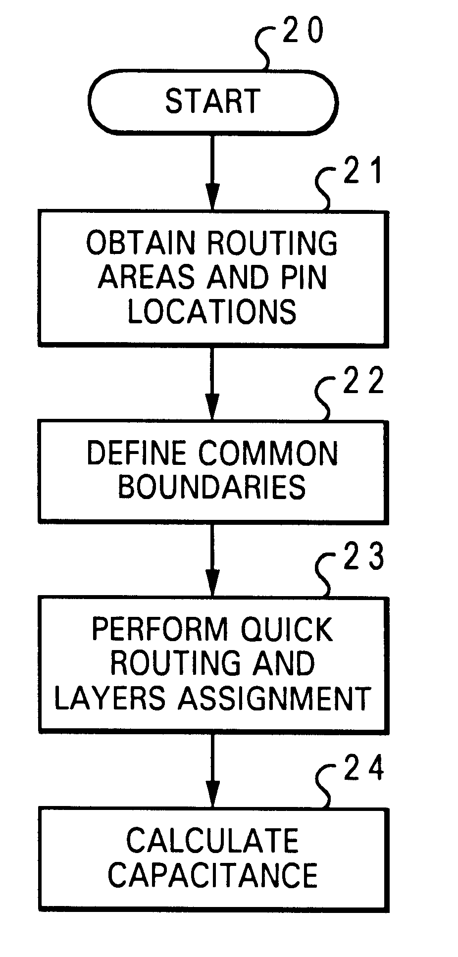
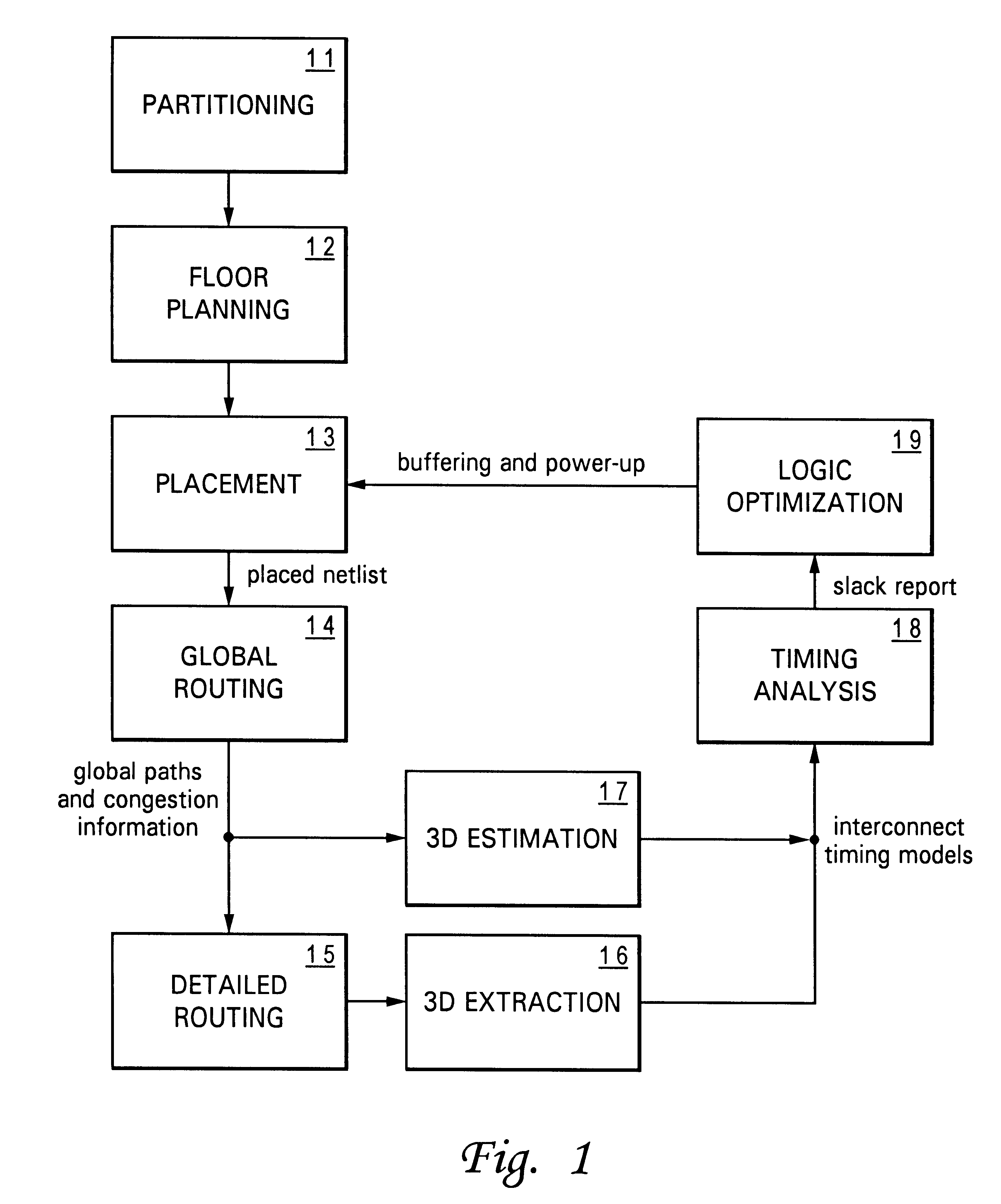
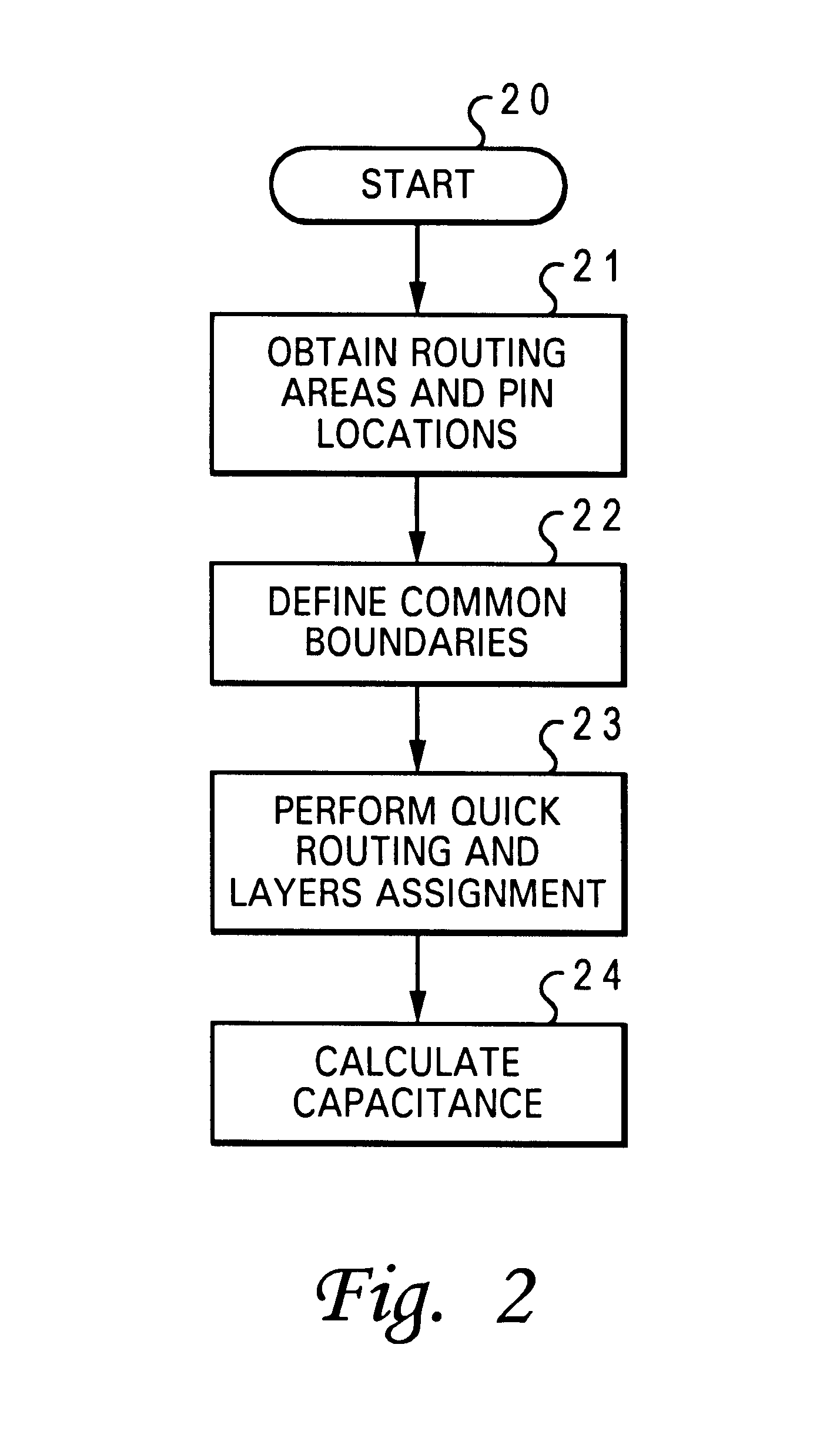
The physical design process for an integrated circuit (IC) is commonly divided into various distinct stages. These stages include Partitioning, Floor Planning, Placement, Routing, etc. Most, if not all, of the design stages can be partially or fully automated utilizing Computer-Aided Design (CAD) tools.

Referring now to the drawings and, in particular, to FIG. 1, there is illustrated a high-level logic flow diagram of various stages in an IC design process. An IC design may contain several million transistors, and layout of the entire IC in a single setting is almost impossible due to the limitation of memory space as well as the computation power available. Therefore, the IC design is normally partitioned by grouping all electronic components within the IC design into blocks, such as sub-circuits and modules, during a Partitioning stage, as shown in block 11. The actual Partitioning step considers many factors such as size of blocks, number of blocks, and number of interconnections ...


PUM


Abstract

A method for performing capacitance estimations on an integrated circuit design routed by a global routing tool is disclosed. Routing areas and pin locations of a net within an integrated circuit design are initially obtained from a global routing tool. Common boundaries among the routing areas are then defined. Before the performance of a detailed routing step, congestion information furnished by the global routing tool is utilized to perform probabilistic capacitance calculations for an interconnect that can be routed within the routing areas via the defined common boundaries to connect the pin locations.

Description

1. Technical FieldThe present invention relates to data processing in general and, in particular, to a method and system for performing capacitance estimations on an integrated circuit design. Still more particularly, the present invention relates to a method and system for performing capacitance estimations on an integrated circuit design that is routed utilizing a global routing tool.2. Description of the Prior ArtA microelectronic integrated circuit (IC) typically comprises a large number of electronic components that are fabricated by layering several different materials on a silicon wafer. Signals are communicated among these electronic components via interconnects. Thus, path delays in an IC are typically dominated by the signal propagation time of interconnects within the IC. In order to properly estimate the signal propagation time of interconnects within an IC during its design, it is crucial to determine the electrical characteristics (including distributed capacitance and...

Claims


Application Information

Patent Timeline
IPC IPC(8): G06F17/50
CPCG06F17/5036G06F30/367
Inventor MEHROTRA, SHARADPATEL, PARSOTAM TRIKAM
Owner IBM CORP
Why Eureka
Try Eureka