Method and apparatus for reducing wafer to wafer deposition variation

a technology of deposition variation and reducing wafers, which is applied in the direction of individual semiconductor device testing, semiconductor/solid-state device testing/measurement, instruments, etc., can solve the problems of inability to accurately measure the deposition rate of cvd tools, affecting the deposition rate, and cvd tools are subject to numerous idle times

Inactive Publication Date: 2002-07-09
ADVANCED MICRO DEVICES INC
View PDF3 Cites 53 Cited by
  • Summary
  • Abstract
  • Description
  • Claims
  • Application Information

AI Technical Summary

Problems solved by technology

As the CVD tool is used repeatedly, material builds up on the internal surfaces of the tool, eventually affecting the deposition rate.
The CVD tool is subject to numerous idle times, including the times preventative maintenance is performed, where the temperature of the tool is maintained at a level significantly less than its operating temperature.
Other reasons for idle time include periodic testing or calibration and delays caused by other tools (not shown) upstream in the processing line.
When the tool is brought back into service after an idle period, there is inherent variability in the deposition rate of the tool due to changes in the thermal characteristics of the tool.
This rework is costly because it ties up the tools necessary for the rework to process only a limited number of wafers.
Adjusting the temperature, as described above, has precision limitations.
First, the large thermal mass of the tool causes stability problems for the changing temperatures.
Thus, the inherent inaccuracy of the thermocouple for this fine of a temperature change also adds instability to the system.
These instabilities increase the likelihood that the thickness of the deposited layer will not be within acceptable limits and the wafer will require rework.

Method used


Image

  • Method and apparatus for reducing wafer to wafer deposition variation
  • Method and apparatus for reducing wafer to wafer deposition variation
  • Method and apparatus for reducing wafer to wafer deposition variation

Examples


Embodiment Construction

Illustrative embodiments of the invention are described below. In the interest of clarity, not all features of an actual implementation are described in this specification. It will of course be appreciated that in the development of any such actual embodiment, numerous implementation-specific decisions must be made to achieve the developers' specific goals, such as compliance with system-related and business-related constraints, which will vary from one implementation to another. Moreover, it will be appreciated that such a development effort might be complex and time-consuming, but would nevertheless be a routine undertaking for those of ordinary skill in the art having the benefit of this disclosure.

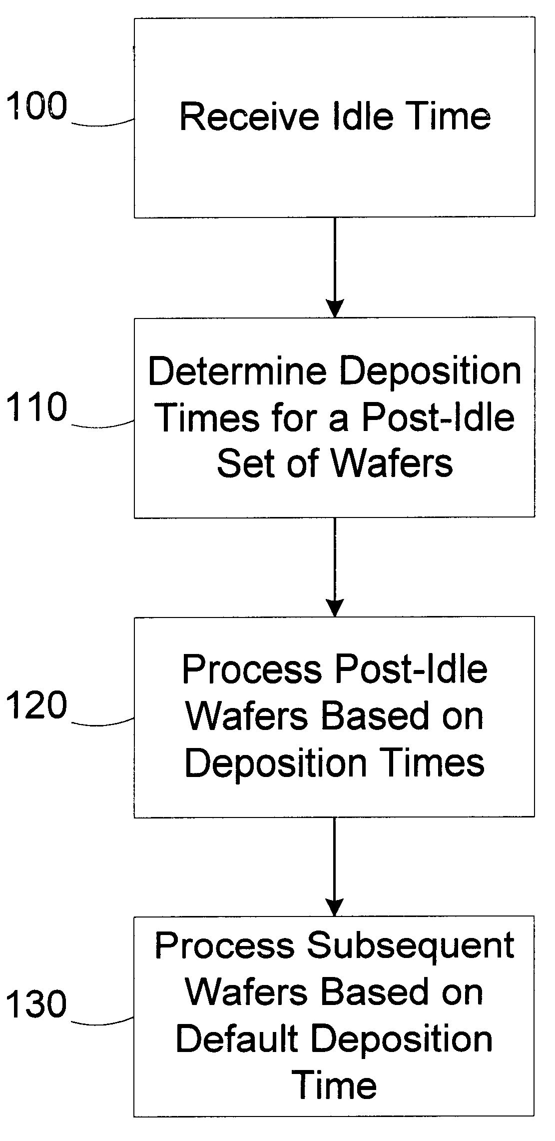
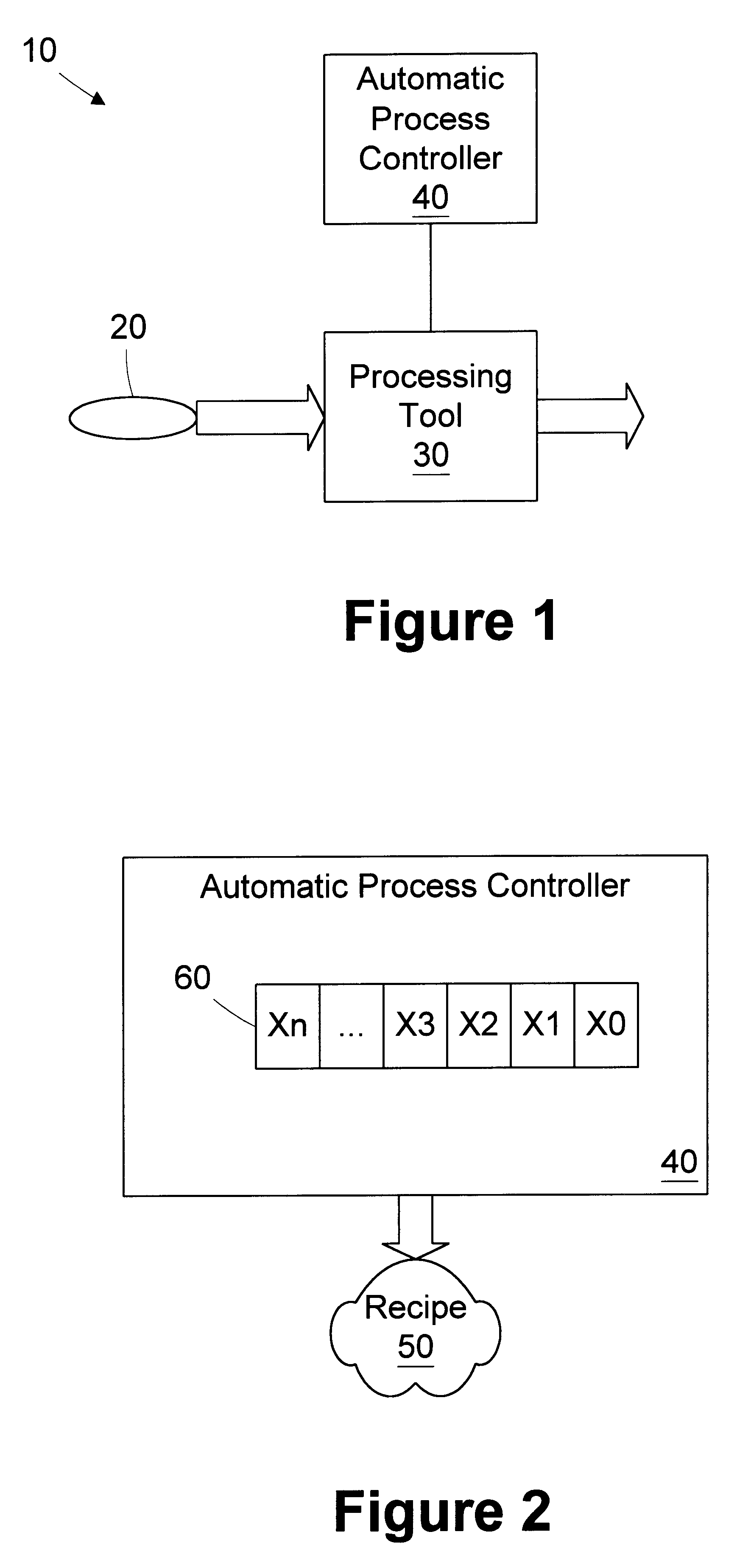
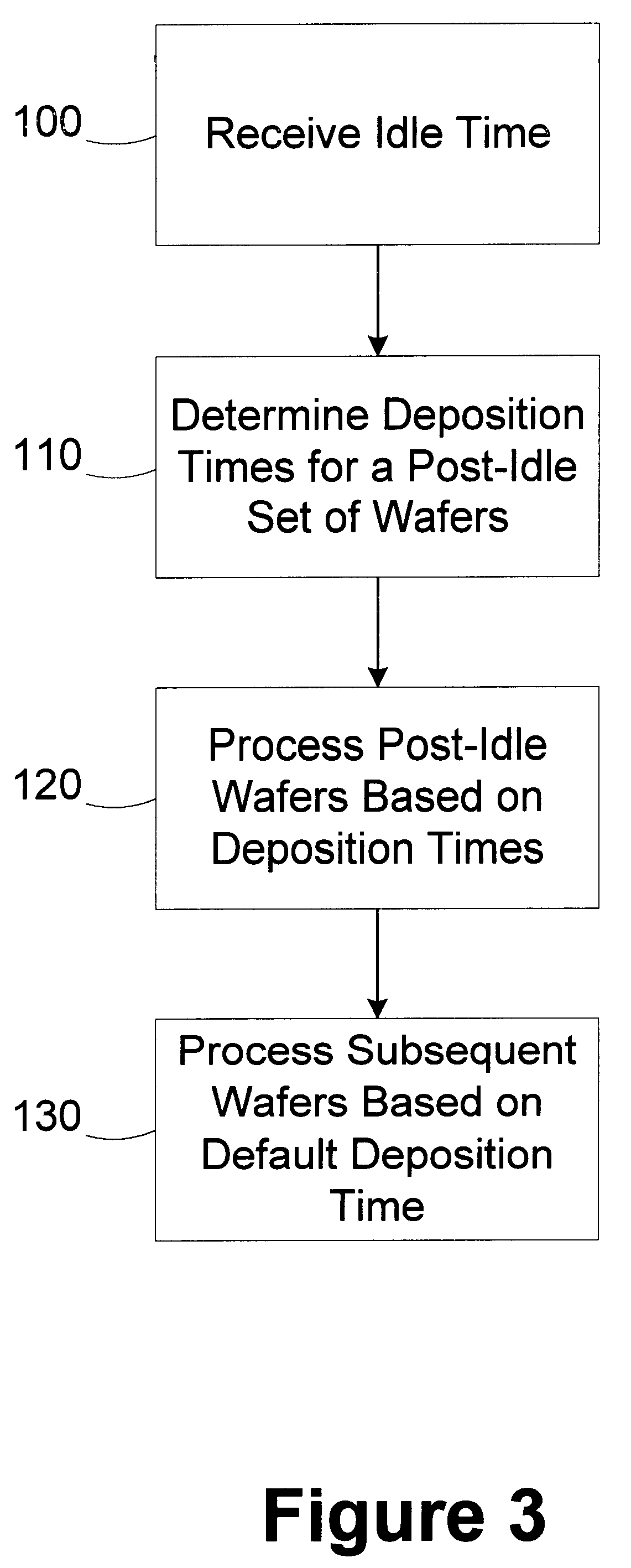
Referring now to the figures, and in particular, to FIG. 1, a simplified diagram of a processing line 10 for processing wafers 20 in accordance with the present invention is provided. The processing line 10 includes a processing tool 30, and an automatic process controller 40. The auto...


PUM

PropertyMeasurementUnit
temperatureaaaaaaaaaa
thicknessesaaaaaaaaaa

Abstract

A processing line includes a processing tool and an automatic process controller. The processing tool is adapted to deposit a layer of material on a semiconductor wafer based on an operating recipe. The automatic process controller is adapted to identify a post-idle set of wafers to be processed in the processing tool after an idle period, determine deposition times for wafers in the set of post-idle wafers, and modify the operating recipe of the processing tool for each of the wafers in the post-idle set based on the deposition times. A method for reducing wafer to wafer deposition variation includes designating a set of post-idle wafers; determining a deposition time for each of the wafers in the post-idle set, at least two of the deposition times being different; and depositing a layer on the wafers in the post-idle set based on the deposition times determined.

Description

1. Field of the InventionThis invention relates generally to semiconductor device manufacturing, and more particularly, to a method and apparatus for reducing wafer to wafer deposition variation.2. Description of the Related ArtIn the manufacture of semiconductor devices, wafers, such as silicon wafers, are subjected to a number of processing steps. The processing steps include depositing or forming layers, patterning the layers, and removing portions of the layers to define features on the wafer. One such process step is the formation of a layer by chemical vapor deposition (CVD), where reactive gases are introduced into a vessel, e.g. a CVD tool, containing the semiconductor wafers. The reactive gases facilitate a chemical reaction that causes a layer to form on the wafers.As the CVD tool is used repeatedly, material builds up on the internal surfaces of the tool, eventually affecting the deposition rate. Preventative maintenance procedures are performed periodically to remove thi...

Claims


Application Information

Patent Timeline
Patent Type & Authority Patents(United States)
IPC IPC(8): H01L21/66
CPCH01L22/20Y10S414/135
Inventor LAM, KIN-SANGSUN, SEY-PING
Owner ADVANCED MICRO DEVICES INC
Why Eureka
Try Eureka