Display device including a transparent electrode pattern covering and extending along gate & source lines
a technology of transparent electrodes and electrodes, which is applied in the direction of load-engaging elements, instruments, travelling gear, etc., can solve the problems of reducing the effective area of a pixel and darkening the screen
- Summary
- Abstract
- Description
- Claims
- Application Information
AI Technical Summary
Benefits of technology
Problems solved by technology
Method used
Image
Examples
first embodiment
[First Embodiment]
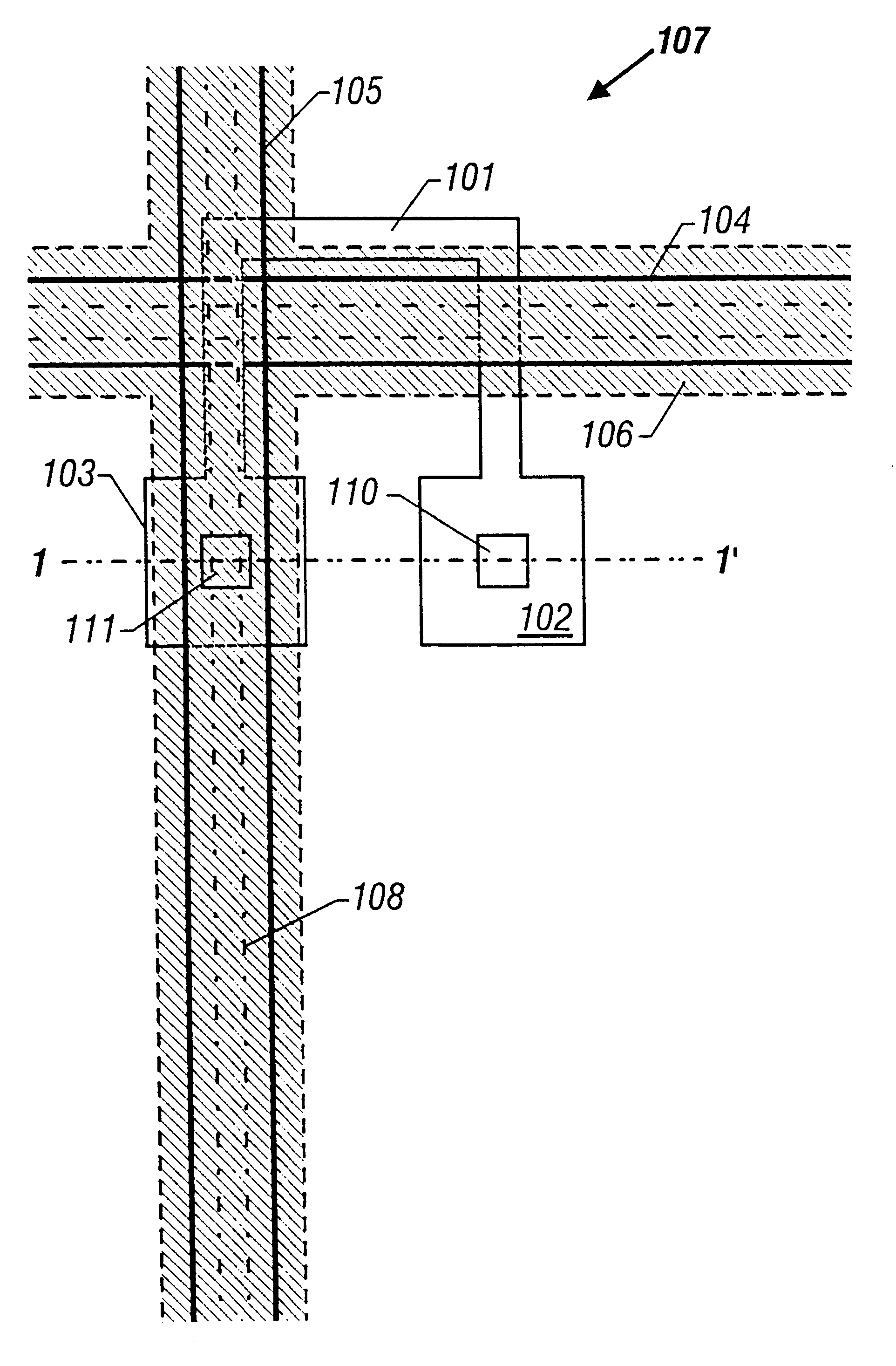
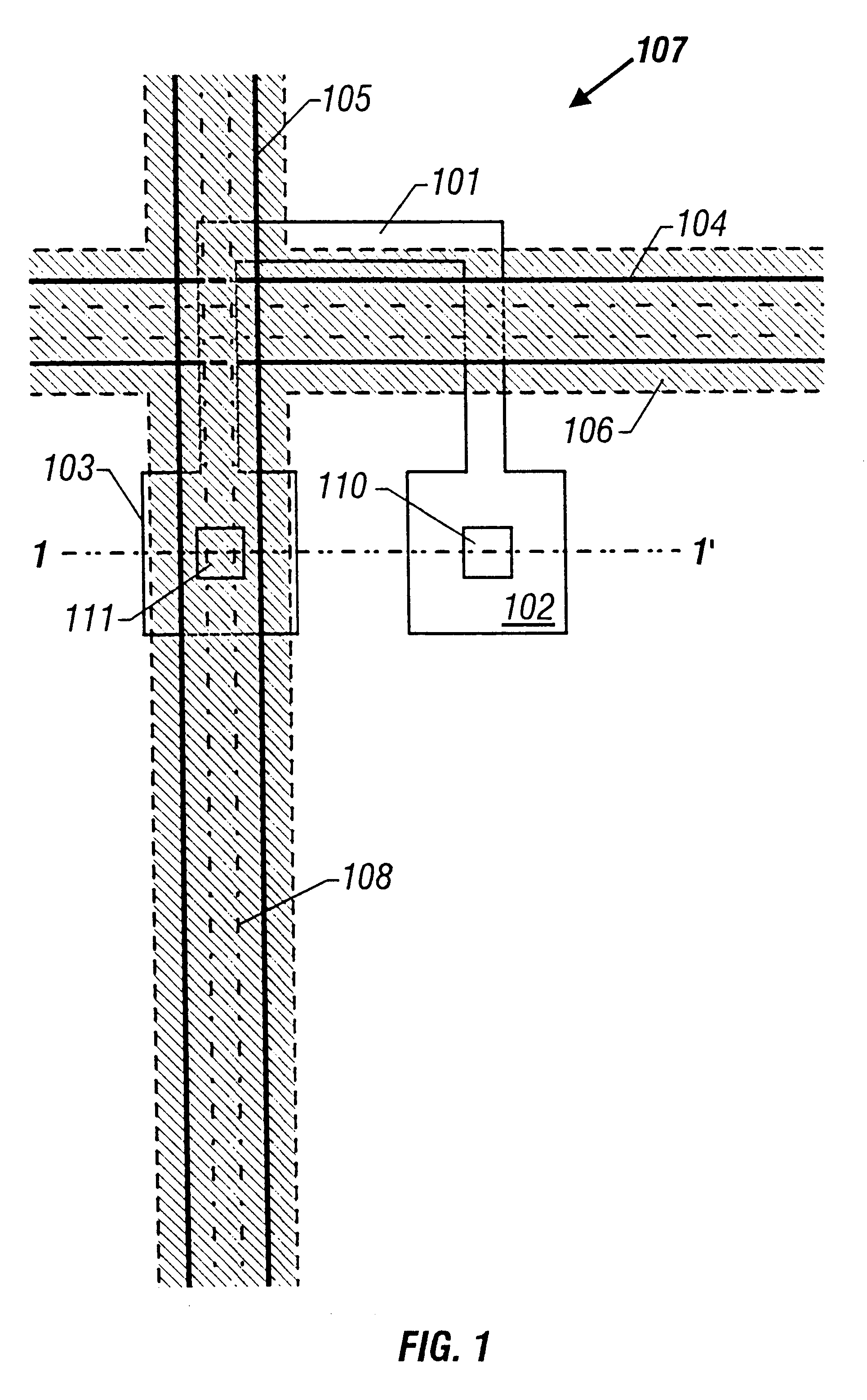
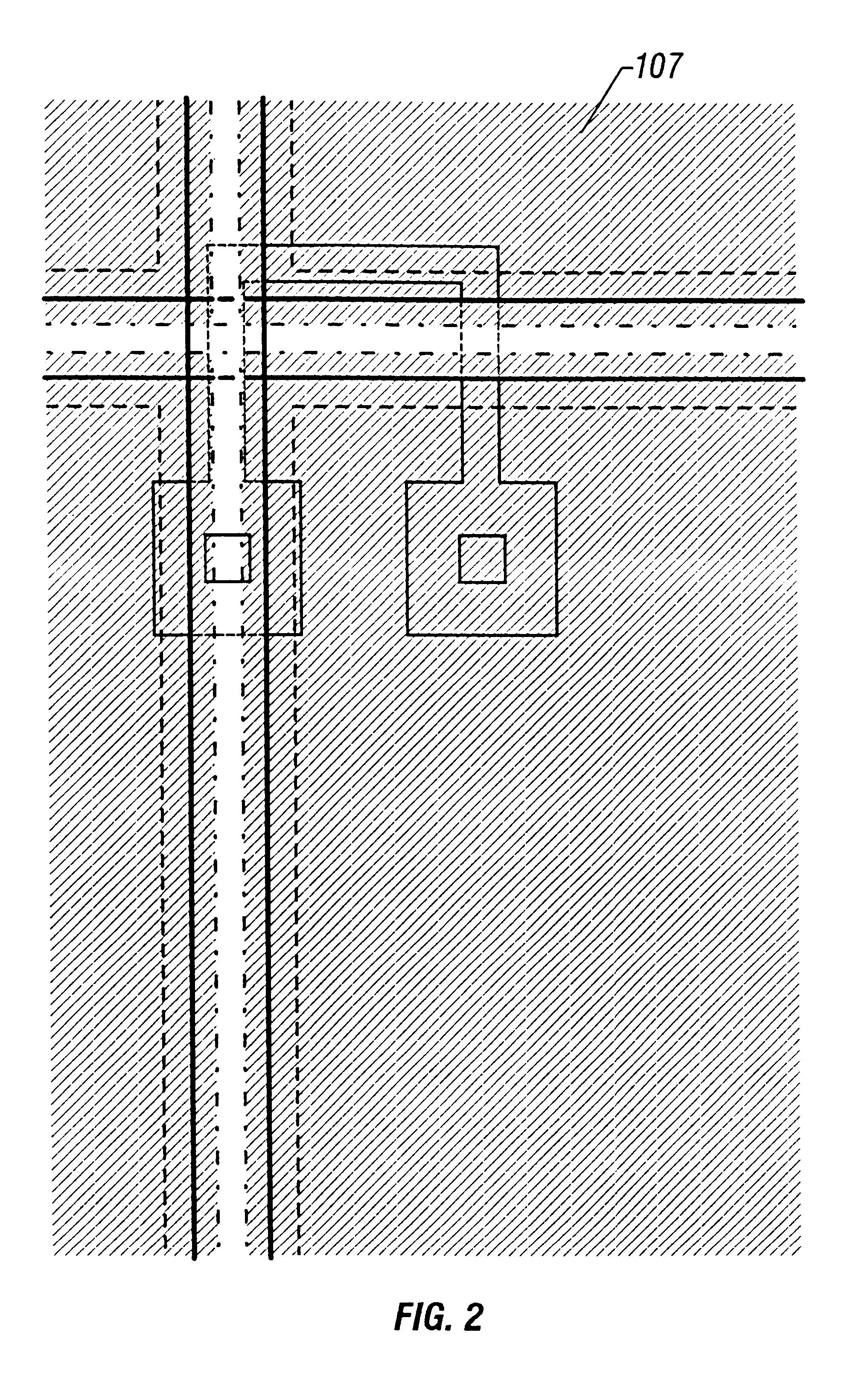
FIGS. 1 through 3 show the structure of the present embodiment. FIGS. 1 through 3 are enlarged plan views showing part of one pixel of an active matrix type liquid crystal display.
FIGS. 1 through 3 show the same part. The structure thereof will be explained with reference to FIG. 1 at first. In FIG. 1, a pattern 101 constitutes an active layer of a thin film transistor. The active layer 101 is made of a crystal silicon film.
A reference numeral 102 which is part of the active layer 101 is a region called as a drain region. A reference numeral 103 is a region called as a source region. These regions are N-type in case of N-channel type and are P-type in case of P-channel type.
A pattern 104 is a gate line. Regions in the active layer 101 at the part where the gate line 104 overlaps with the active layer 101 are channel regions. Regions where the gate line 104 overlaps with the active layer 101 function as gate electrodes.
A source line 105 contacts with the source regi...
second embodiment
[Second Embodiment]
The present embodiment relates to a structure modified from have been overlapped with the pixel electrode and the overlap regions have been caused to function as the black matrix in the structure shown in the first embodiment. The structure shown in the first embodiment has been useful in increasing the aperture ratio to the maximum. However, it is necessary to increase the area of the black matrix depending on a requested image quality or a displaying method.
The present embodiment relates to a structure which can be utilized in such a case. FIG. 11 shows a section of a pixel part according to the present embodiment. FIG. 11 corresponds to FIG. 10 and the same reference numerals with those in FIG. 10 denote the same components in FIG. 11.
In the present embodiment, part of a film 1102 which is made of a titanium film or chromium film (or an adequate metallic film) and which constitutes the black matrix overlaps with the edge of the pixel electrode 107 made of ITO.
A...
PUM
| Property | Measurement | Unit |
|---|---|---|
| thickness | aaaaa | aaaaa |
| thickness | aaaaa | aaaaa |
| thickness | aaaaa | aaaaa |
Abstract
Description
Claims
Application Information
 - R&D
- Intellectual Property
- Life Sciences
- Materials
- Tech Scout
- Unparalleled Data Quality
- Higher Quality Content
- 60% Fewer Hallucinations
Browse by: Latest US Patents, China's latest patents, Technical Efficacy Thesaurus, Application Domain, Technology Topic, Popular Technical Reports.
© 2025 PatSnap. All rights reserved.Legal|Privacy policy|Modern Slavery Act Transparency Statement|Sitemap|About US| Contact US: help@patsnap.com


