Wavelength multiplexer and optical unit
a multiplexer and optical unit technology, applied in the field of wavelength multiplexers and optical units, can solve the problems of large loss, scattered reflected light, and inability to couple reflected light well with the optical waveguide 2, and achieve the effect of minimizing the increase of loss in the optical uni
- Summary
- Abstract
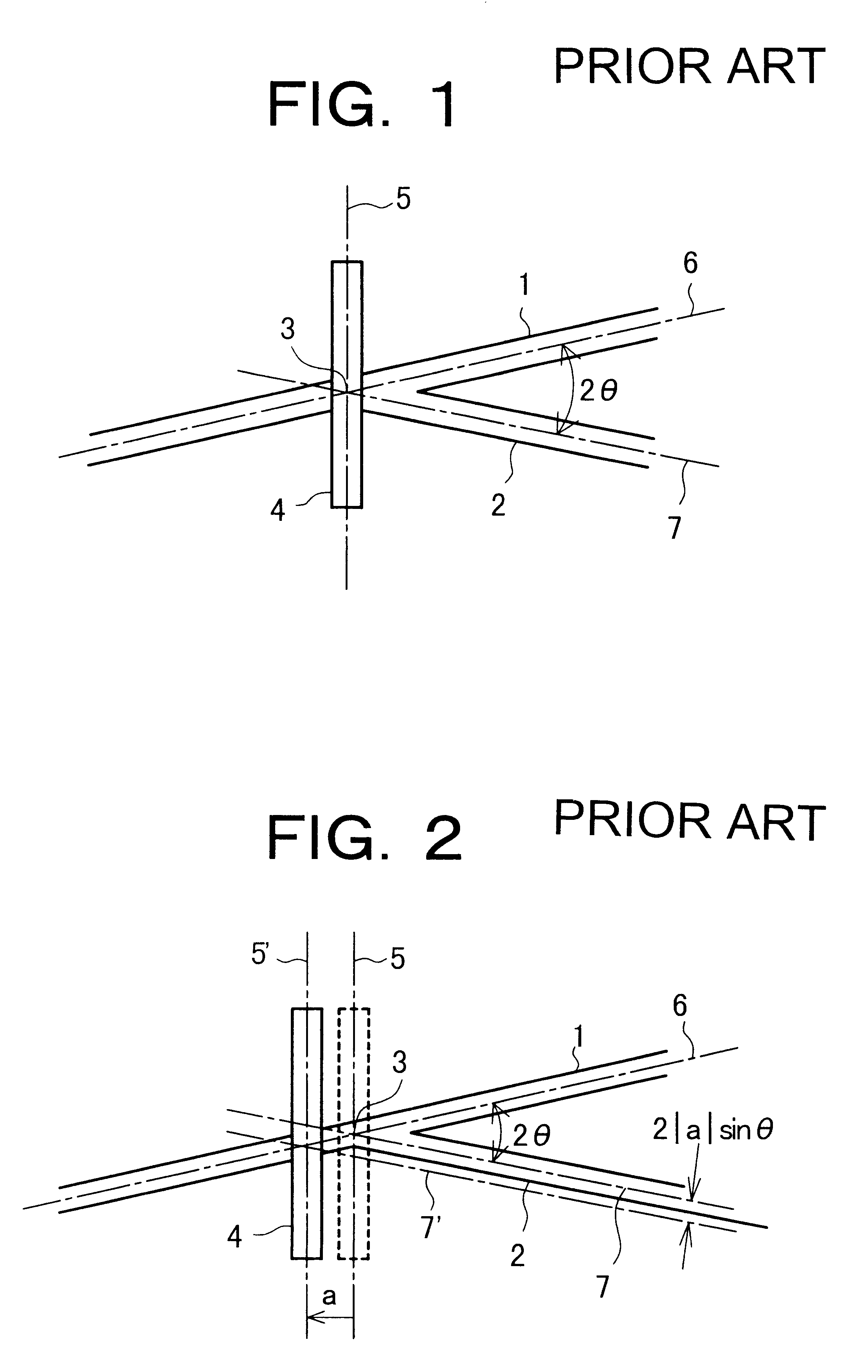
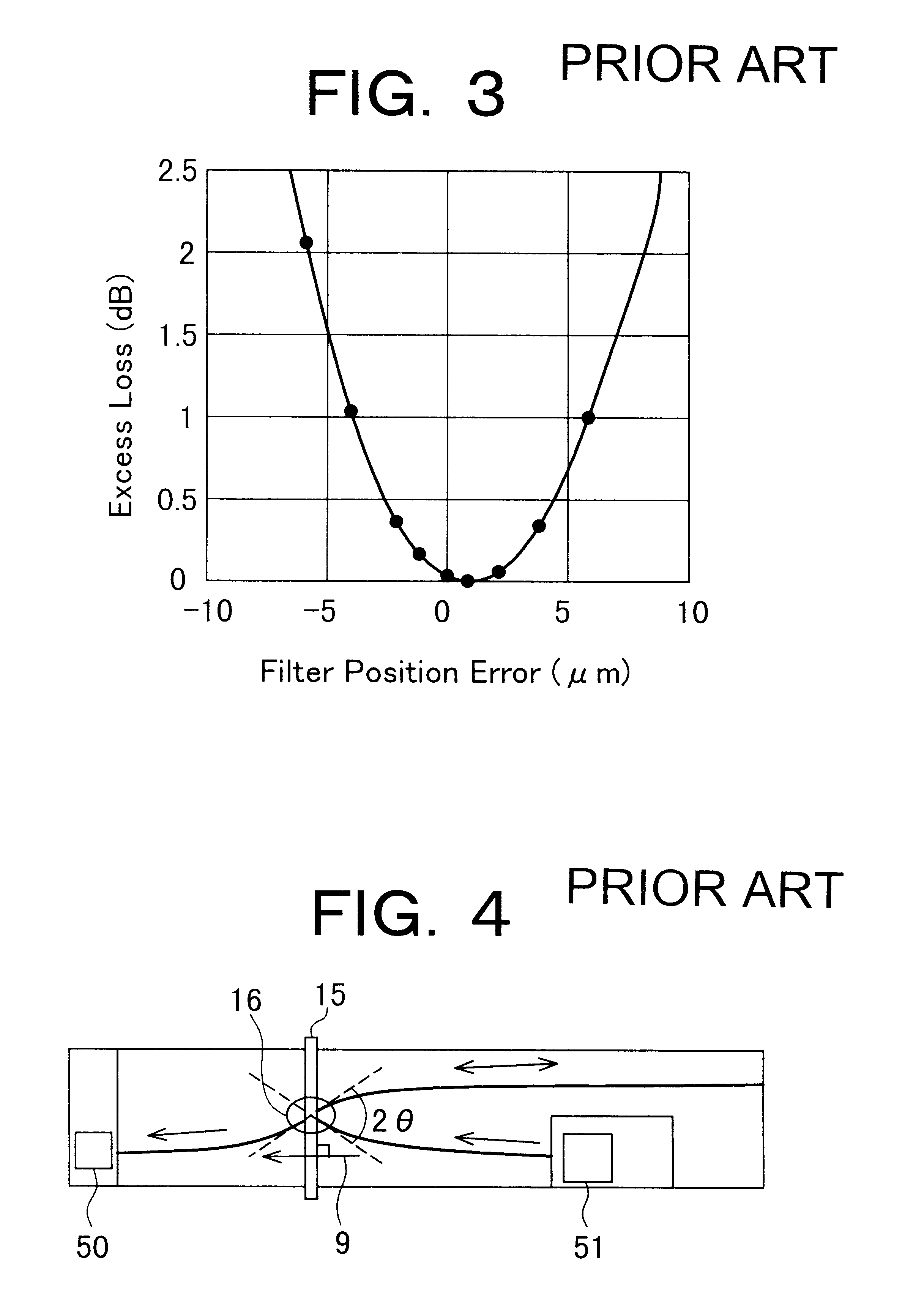
- Description
- Claims
- Application Information
AI Technical Summary
Benefits of technology
Problems solved by technology
Method used
Image

Examples
first embodiment
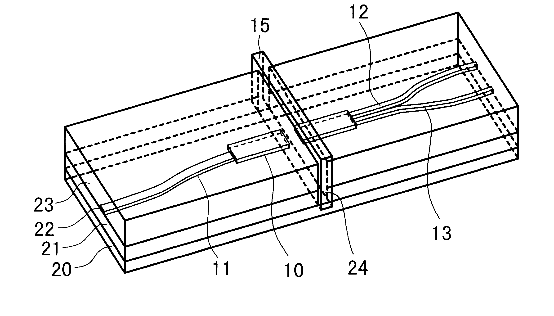
FIG. 8 is a perspective view showing a wavelength multiplexer according to the present invention and FIG. 9 is an enlarged plan view of a wavelength combining / branching section thereof.
An optical waveguide is formed on a predetermined substrate, say, a silicon (Si) substrate 20, using two kinds of fluorinated polyimide resins different in refractive index. This optical waveguide includes at least a first clad layer 21, a core area 22, and a second clad layer 23. The numeral 24 denotes a slot for insertion of a filter therein. For example, the first, or lower, clad layer 21, the core 22, and the second, or upper, clad layer 23 are 5 82 m, 6.5 .mu.m, and 15 .mu.m, respectively, in thickness. A core to clad refractive index ratio is set at 0.3%. The wavelength combining / branching section includes at least a multi-mode interference type optical waveguide 10, a first optical waveguide 11, a second optical waveguide 12, and a third optical waveguide 13. The width W and length L of the mul...
third embodiment
FIG. 15 is a perspective view of an optical transceiver module according to the present invention. This embodiment shows an example in which, in an optical unit having optical waveguides according to the present invention both light emitting element and light receiving element are mounted on a single substrate. This configuration is easy to use and useful as a practical mode of an optical transceiver.
In this third embodiment, a photo-diode 51 as a light receiving element and a laser diode 50 as a light emitting element are mounted on the silicon substrate 20 of the wavelength multiplexer described in the previous first embodiment. More specifically, on the silicon substrate 20 is formed a multi-layer film of polymer as is the case with the previous embodiments. Then, the polymer is removed at predetermined portions, allowing the Si substrate 20 to be exposed at the predetermined portions. The conventional dry-etching technique will do for the removal of the polymer. First electrodes...
fifth embodiment
FIG. 18 is a plan view showing a basic configuration of an optical receiver module according to the present invention. In this optical reception module to which the invention is applied, a multi-wavelength signal light is branched wavelength by wavelength and the thus-branched signal lights are received by light receiving elements suitable for the respective wavelengths.
According to a basic configuration of this embodiment, a light signal provided from an optical fiber 65 is filtered into desired wavelengths by two filters 63 and 64 and selected wavelengths of lights are detected by light receiving elements 62-1, 62-2, 62-3, 62-4, 62-5 and 65-6 which are disposed on the transmission sides of the filters.
Referring to FIG. 18, plural wavelength multiplexers 60 and optical waveguides 61 which connect them are formed on a silicon substrate as is the case with previous examples, and plural photo-diodes 62-1, 62-2, 62-3, 62-4, 62-5 and 62-6 are disposed on transmission-side end faces of t...
PUM
 Abstract
Description
Claims
Application Information