Optimization of printed wire circuitry on a single surface using a circle diameter

a printed wire circuit and circle diameter technology, applied in the field of routing and sizing of printed wire circuitry, can solve the problems of not addressing itself to the problem of obtaining optimized printed wire width, not addressing itself to the optimization of wire width and spacing, and not addressing the optimization of spacing between conductors

Inactive Publication Date: 2002-09-03
IBM CORP
View PDF15 Cites 0 Cited by
  • Summary
  • Abstract
  • Description
  • Claims
  • Application Information

AI Technical Summary

Problems solved by technology

Although numerous publications are currently available which direct themselves to the routing and spacing of printed wires on surfaces, for instance, such as on single surface or multiple surfaces of semiconductor devices, these do not address themselves to the problem of obtaining optimized printed wire widths and spacings in correlation with the amount of available spacing across a particular surfaces onto which the wires are to be applied.
Chang U.S. Pat. No. 5,581,098 discloses circuit routing structure in a multi-layer product and does not address itself to the optimization of interconnect wire widths and spacings or positioning thereof on an available surface

Method used


Image

  • Optimization of printed wire circuitry on a single surface using a circle diameter
  • Optimization of printed wire circuitry on a single surface using a circle diameter
  • Optimization of printed wire circuitry on a single surface using a circle diameter

Examples


Embodiment Construction

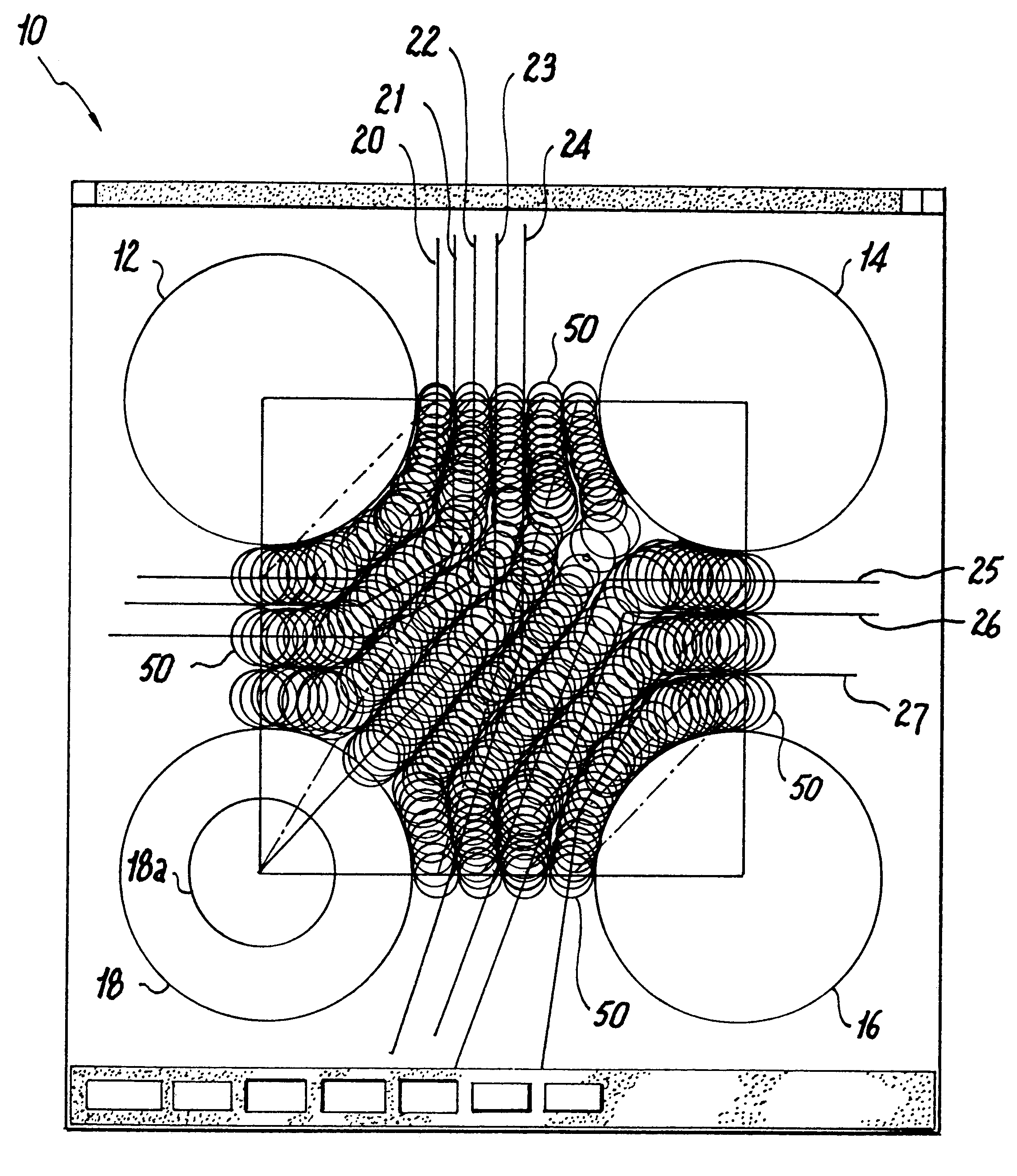
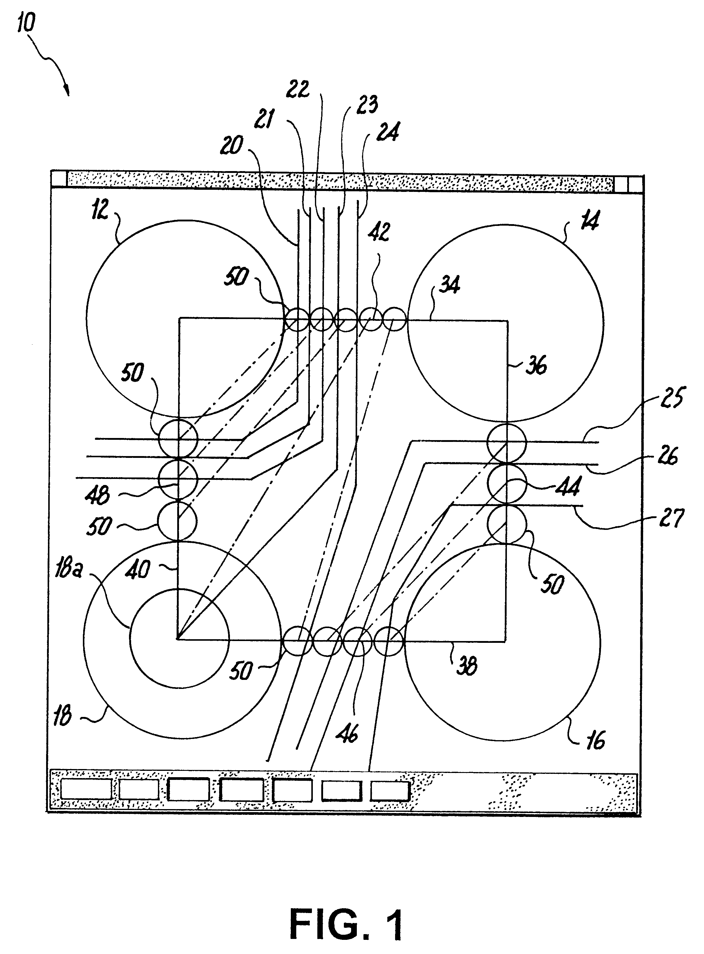
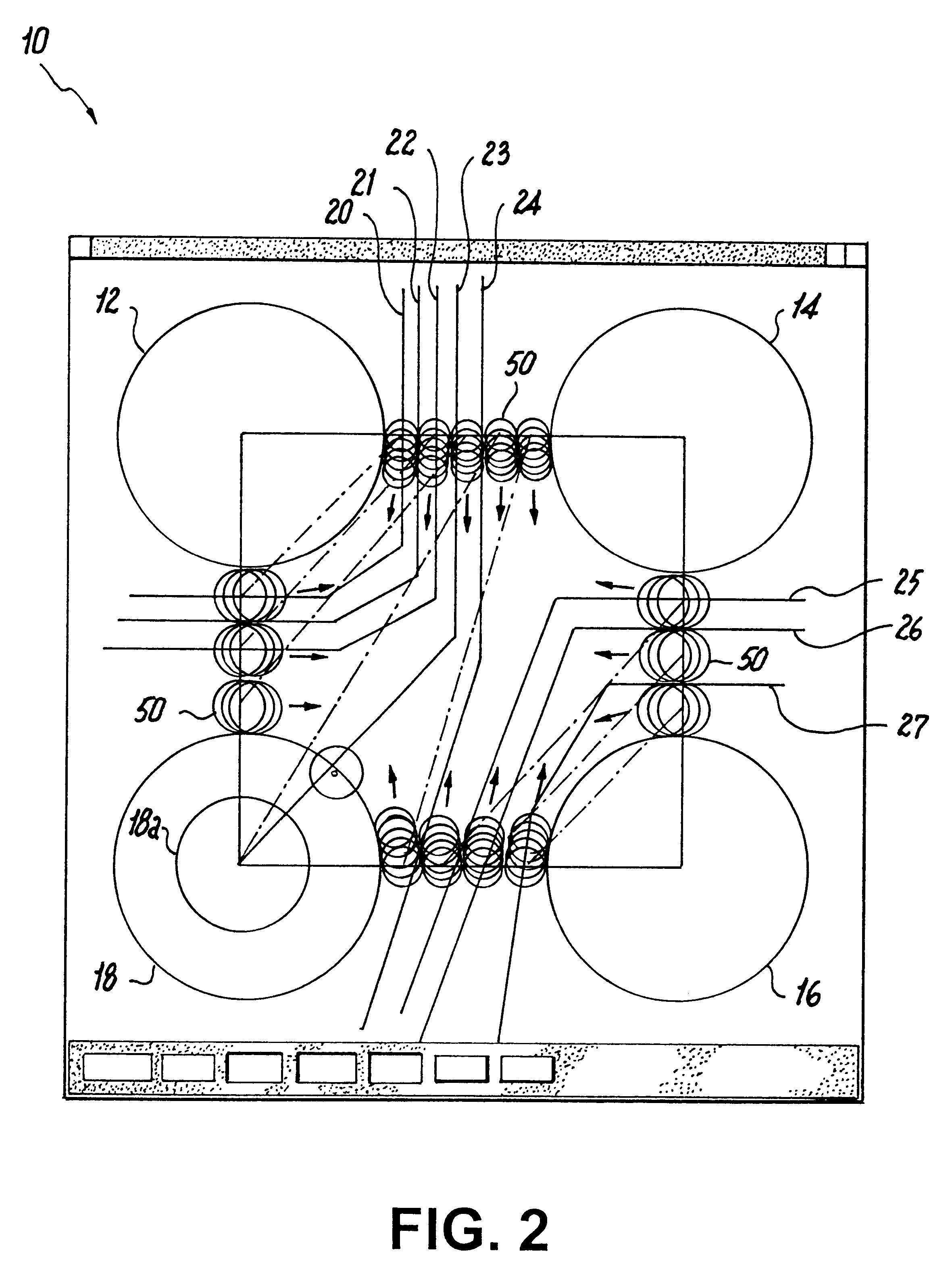
Referring now in specific detail to the drawings, as illustrated in FIG. 1 there is shown a computer representation of a surface 10 which may be considered to be the area of a semiconductor device. Arranged within the surface are a plurality of lands 12, 14, 16 and 18, or other regions which; for example, may be pads 18a for ballgrid arrays (BGAs) which are to be either interconnected by printed wire circuitry, or which form boundaries for passages for the routing of wires therebetween and to provide for suitable wire interconnections.

The algorithm for implementing the optimized routing of circuitry wires which are to be imprinted on the surface may be implemented by detecting where suitable guidelines 20, 21, 22, 23, 24 intersect first border portion 34 of an imaginary border box which is formed as a positioning connection between the various lands or wire paths.

Guide lines 25, 26, 27 intersect a second border portion 36, with all of the above guide lines being plotted to angularly...


PUM


Abstract

A method of routing and sizing of wires in the formation of wiring paths extending through a region. More particularly, the method relates to optimizing the routing and sizing of printed wire circuitry on a single surface, such as on semiconductor devices.

Description

1. Field of the InventionThe present invention relates to a method of routing and sizing of wires in the formation of wiring paths extending through a region; and more particularly, relates to optimizing the routing and sizing of printed wire circuitry on a single surface, such as on semiconductor devices.In the implementation of the positioning and sizing of the printed wire circuitry on semiconductor devices or substrates, an important aspect is to be able to utilize printed wire widths and spacings which are optimized with regard to the amount of available spacing on the surface of the device or substrate. In particular, for fine pitch ballgrid array chip carriers (PBGA) the printed circuitry wire widths and spacings vary in accordance with the amount of space which is available on the device or semiconductor surface. Thus, as the available spacing for the printed wires decreases, in view of the number of wires which must pass between the ballgrid array paths or other converting ...

Claims


Application Information

Patent Timeline
IPC IPC(8): G06F17/50
CPCG06F17/5077G06F30/394
Inventor MALLING, DONALD J.
Owner IBM CORP
Why Eureka
Try Eureka