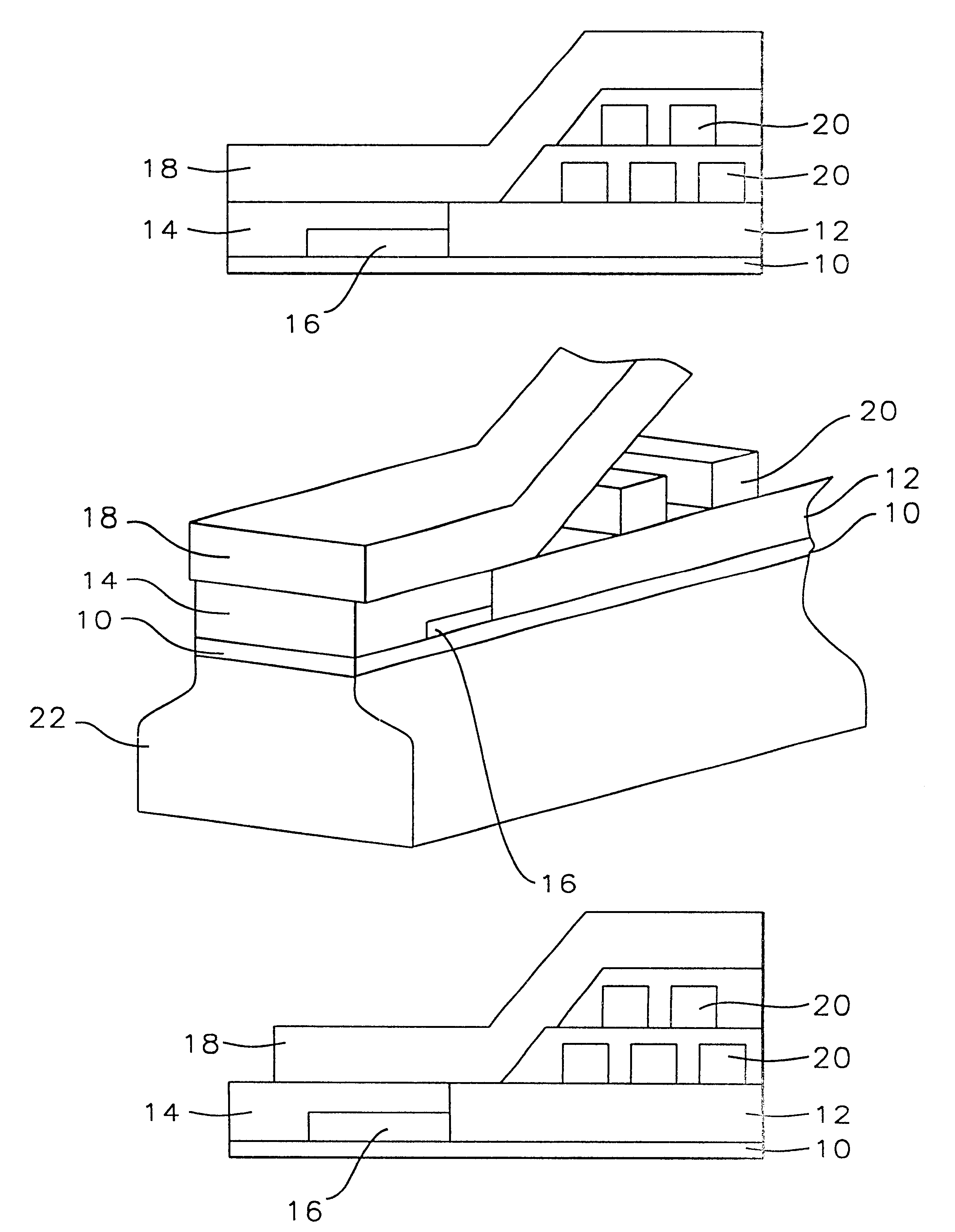
The present invention is a high data-rate stitched pole magnetic write head and a method for fabricating it. This head can be formed as part of a giant magneto-resistive read/write head structure.
A description of the preferred embodiments of this invention will be given in the context of the schematic drawings designated FIG. 1A, FIG. 1B, FIG. 1C, FIG. 1D, FIG. 2, FIG. 3, FIG. 4, FIG. 5, FIG. 6, FIG. 7, FIG. 8 and FIG. 9.
Referring now to FIG. 1A, we see a schematic cross-sectional view of a completed stitched pole magnetic write head fabricated according to a first preferred embodiment of the present invention. In this embodiment, the upper pole yoke portion, P3 (18), has been stitched to the upper pole piece, P2 (14), so that they are not recessed relative to each other (i.e. (18) and (14) are co-planar at the air-bearing surface). The non-magnetic spacer layer (16) is shown and P3, P2 and the spacer layer configuration have been deposited on the write gap layer (10). The induction coils (20) are shown beneath the upper pole yoke as is an insulating layer (12) which abuts P2 and serves as a base for the coil structure. The details of this fabrication process will be given in the context of FIG. 2 through FIG. 9.
FIG. 1B shows a schematic perspective view of the fabrication in FIG. 1A and includes, for completeness, the lower pole piece (22), which can also serve as an upper shield for the giant magneto-resistive read head which is not shown.
FIG. 1C shows a schematic cross-sectional view of a completed stitched-pole magnetic write head fabricated according to a second preferred embodiment of the present invention. This fabrication is identical to that depicted in FIG. 1A, except that the spacer layer (16) and upper pole piece P2 (14) are longer and the upper pole yoke P3 (18) has been stitched so that it is recessed relative to P2 (14).
FIG. 1D shows a schematic perspective view of the fabrication in FIG. 1C and includes, for completeness, the lower pole piece (22), which can also serve as an upper shield for the giant magneto-resistive read head which is not shown.
FIG. 2 shows the first step of the fabrication process leading to the completed fabrication of either FIG. 1A or FIG. 1C. In FIG. 2, the write gap layer (10), which is a dielectric layer of alumina deposited to a thickness of between 800 angstroms and 5000 angstroms, has been coated with a photoresist layer (22) of a thickness between 1.0 microns and 5.0 microns. The photoresist layer will be patterned, exposed and developed to define both the spacer layer and the pole tip structure P2 according to the method used to create self-aligned depositions.
FIG. 3 shows the exposure of the photoresist layer (22) in the spacer layer deposition region (24).
FIG. 4 shows the photoresist layer (22) subsequent to development and removal of the portion defining the spacer layer.
FIG. 5 shows the deposition of the spacer layer (16), which will be a layer of non-magnetic material such as NiCu, Alumina, Ta or PdCu, deposited to a thickness of between 0.3 microns and 0.8 microns and a width between 5.0 microns and 7.0 microns. For the embodiment in which the upper pole yoke is not to be recessed, said spacer layer will have a length between 0.5 microns and 1.0 microns. For the embodiment in which the upper pole yoke is to be recessed, the spacer layer will have a length between 0.5 microns and 1.5 microns.
FIG. 6 shows the removal of the remaining portion of the photoresist layer to expose a region (23) on which the pole tip, P2, will be formed.
FIG. 7 shows the formation of the magnetic pole tip, P2 (14), over said exposed region and the spacer layer. The pole tip can be of magnetic material such as FeN, FeAlN, FeTaN or CoNiFe and will be formed by plating or deposition to a thickness of between 0.5 microns and 3.0 microns and a length between 3.0 microns and 6.0 microns.
FIG. 8 shows the upper pole yoke, P3 (18), stitched to pole tip P2 (14) but, in this embodiment, not recessed relative to P2. The upper pole yoke, P3, may be of magnetic material such as FeN, FeTaN, FeAlN or CoFeV, and be deposited to a thickness of between 1.5 microns and 3.0 microns and will be wider than P2 (14) by approximately 0.5 microns on each side.
FIG. 9 shows the equivalent final step as that depicted in FIG. 8, but now done according to a second preferred embodiment of the invention, in which the spacer layer (16), of non-magnetic material such as NiCu, Alumina, Ta or PdCu, is deposited to a thickness of between 0.3 microns and 0.8 microns, with a width between 5.0 microns and 7.0 microns and a length between 0.5 microns and 1.5 microns. The upper pole piece, P2 (14), which can be of magnetic material such as FeN, FeAlN, FeTaN or CoNiFe is plated on or deposited to a thickness of between 0.5 microns and 3.0 microns and has a width between 3.0 microns and 5.0 microns and a length between 3.0 microns and 6.0 microns. The upper yoke, P3 (18), is stitched to the upper pole piece, P2 (14) and is recessed relative to the air bearing surface of said upper pole piece by a distance of between 0.15 microns and 1.5 microns (19).
As is finally understood by a person skilled in the art, the preferred embodiments of the present invention are illustrative of the present invention rather than limiting of the present invention. Revisions and modifications may be made to materials, structures and dimensions used to form a high data-rate stitched pole magnetic write head and to the methods for fabricating it in accord with the preferred embodiments of the present invention, while still providing a high data-rate stitched pole magnetic write head and a method for fabricating it in accord with the present invention as provided by the appended claims.