Method for testing signal paths between an integrated circuit wafer and a wafer tester

a technology of integrated circuit and tester, which is applied in the direction of individual semiconductor device testing, semiconductor/solid-state device testing/measurement, instruments, etc., can solve the problems of connection failure, distorting test, and often a relatively complicated interconnect structur

Inactive Publication Date: 2002-11-05
FORMFACTOR INC
View PDF22 Cites 89 Cited by
  • Summary
  • Abstract
  • Description
  • Claims
  • Application Information

AI Technical Summary

Benefits of technology

It is another object of the invention to provide means for measuring resistance of signal paths thro

Problems solved by technology

Thus the interconnect structure is often a relatively complicated structure including more than one interconnected signal routing layer.
A connection failure may arise, for example, due to a misalignment of pogo pins or probes with their intended contact points, a broken, missing or contaminated pogo pin, probe or contact pad, a misalignment between contact structures within internal layers within the interconnect structure, an open circuit or short circuit fault between conductors within the interconnect structure or within the test head, or defective or missing discrete components in the signal paths through the interconnect structure.
Contactor assemblies are usually designed to provide signal paths having particular resistances, and any variation from the intended resistance, due for exampl

Method used


Image

  • Method for testing signal paths between an integrated circuit wafer and a wafer tester
  • Method for testing signal paths between an integrated circuit wafer and a wafer tester
  • Method for testing signal paths between an integrated circuit wafer and a wafer tester

Examples


Embodiment Construction

)

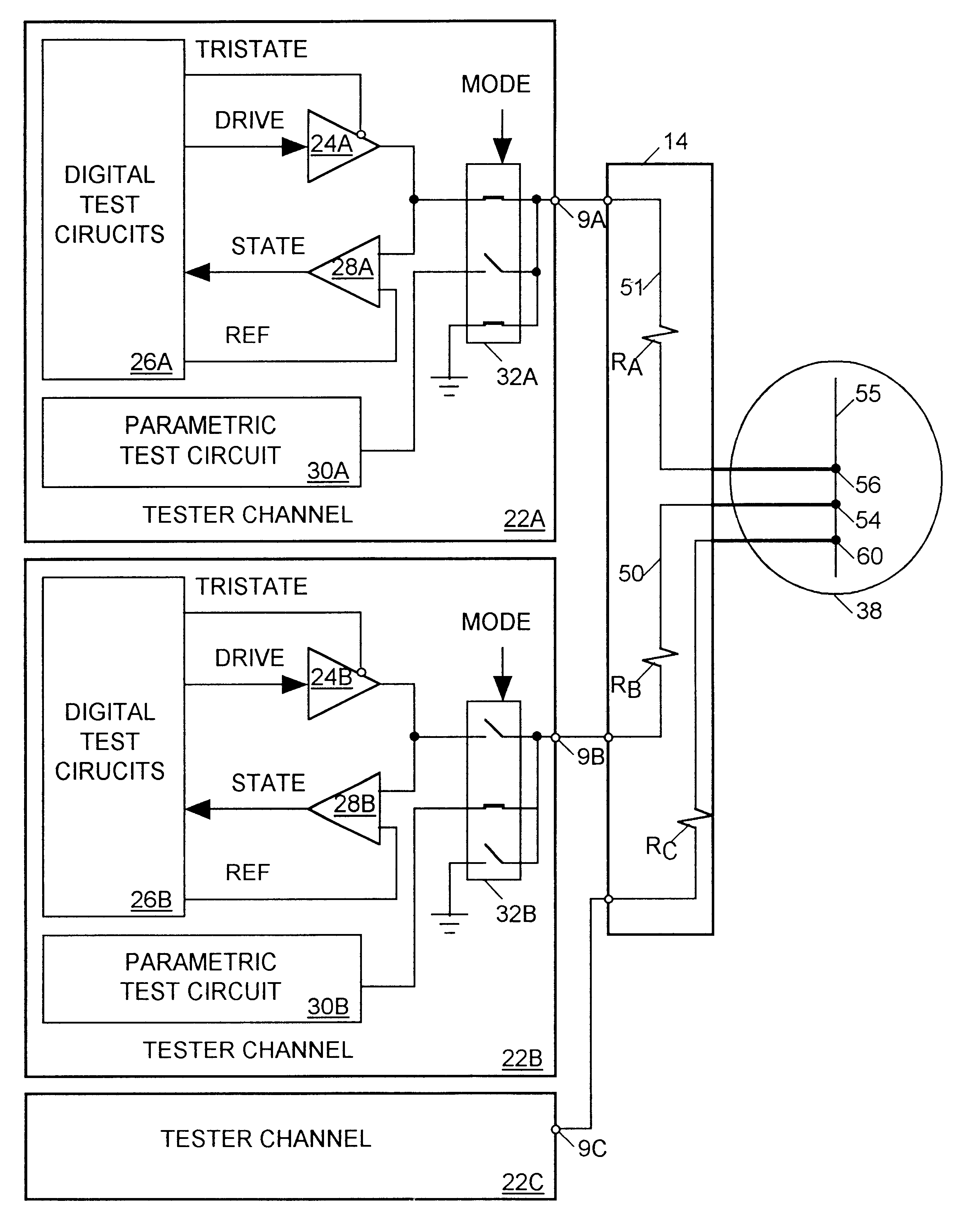
The present invention relates to a method and apparatus for testing signal paths through any kind of interconnect structure for conveying signals between input / output (I / O) ports of a wafer level integrated circuit (IC) tester and test points on an IC wafer to be tested. Since the nature of the invention is best understood in the context of an IC tester architecture, a typical IC tester architecture is briefly outlined below.

Integrated Circuit Tester

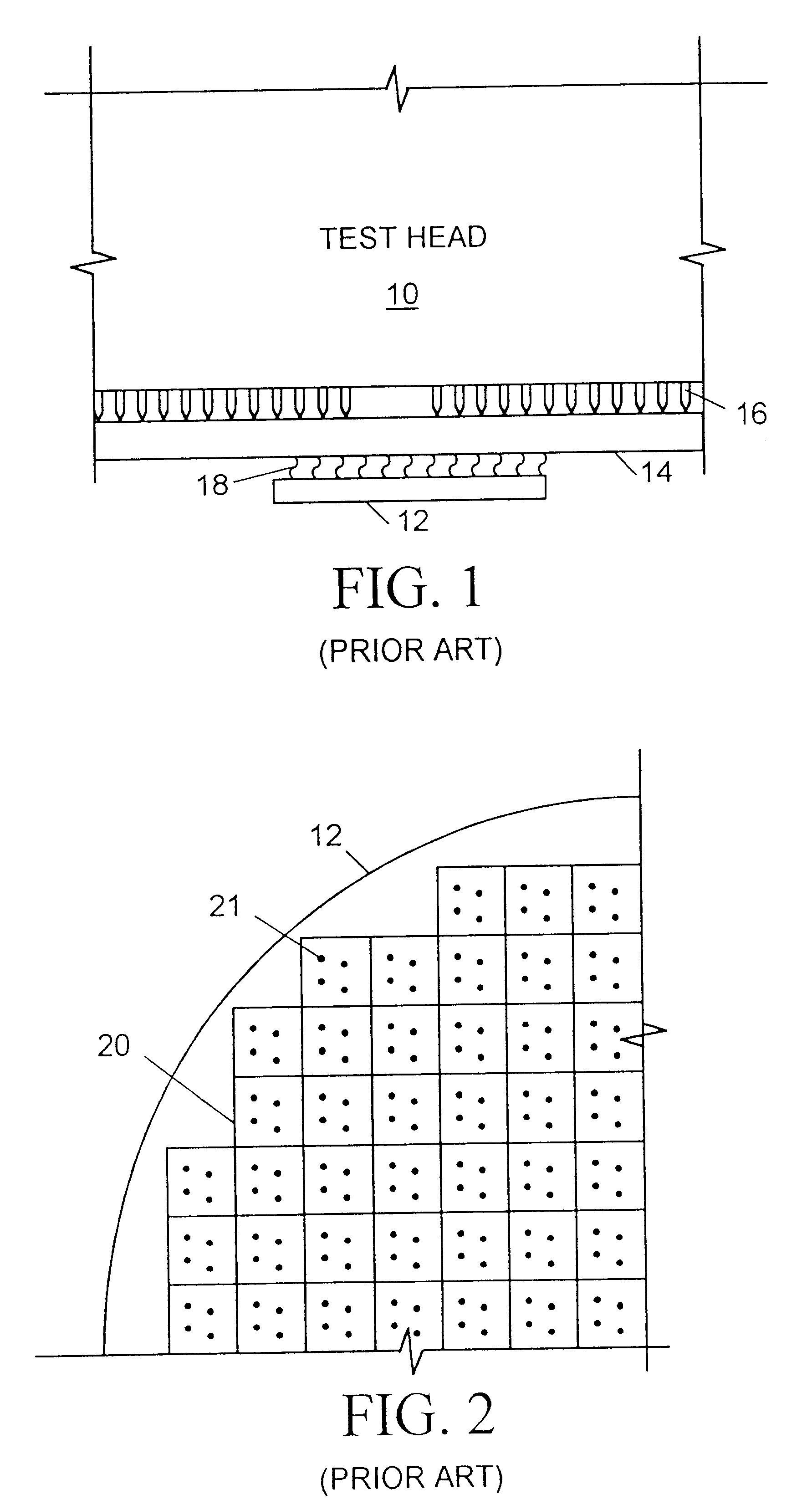
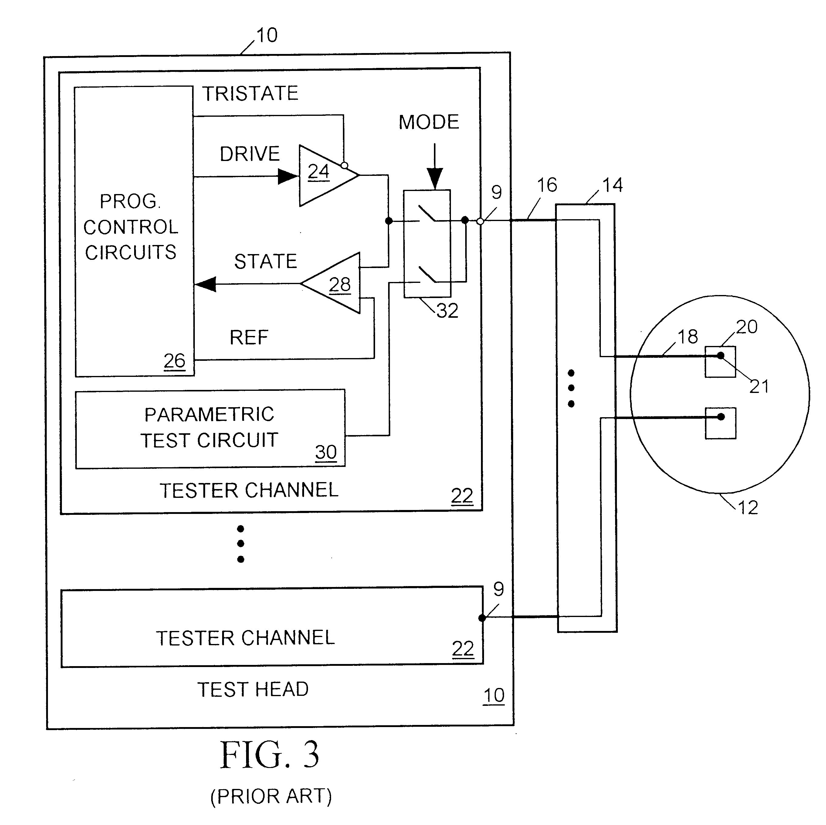
FIG. 1 is a simplified partial elevation view of a test head 10 of a typical prior art IC tester accessing test points on a wafer under test 12 via a conventional interconnect structure 14. FIG. 2 is a plan view of a portion of a wafer 12, and FIG. 3 is a simplified block diagram representing tester circuits mounted in test head 10 of FIG. 1. Referring to FIGS. 1-3, test head 10 holds a set of circuit boards implementing circuits for carrying out both digital and analog tests on ICs implemented in the form of die 20 on wafer 12. In this...


PUM


Abstract

Signal paths within an interconnect structure linking input/output (I/O) ports of an integrated circuit (IC) tester and test points of an IC die on a wafer are tested for continuity, shorts and resistance by using the interconnect structure to access a similar arrangement of test points on a reference wafer. Conductors in the reference wafer interconnect groups of test points. The tester may then test the continuity of signal paths through the interconnect structure by sending test signals between pairs of its ports through those signal paths and the interconnecting conductors within the reference wafer. A parametric test unit within the tester can also determine impedances of the signal paths through the interconnect structure by comparing magnitudes of voltage drops across pairs of its I/O ports to magnitudes of currents it transmits between the I/O port pairs.

Description

1 Field of the InventionThe present invention relates in general to wafer-level integrated circuit (IC) testers, and in particular to a method for verifying signal paths through a structure interconnecting an IC tester to an IC wafer to be tested.2 Description of Related ArtMany integrated circuit (IC) testers test ICs while the ICs are still in the form of die on a semiconductor wafer. A typical wafer tester includes a chassis called a "test head" containing printed circuit boards implementing the circuits that test a wafer. The test circuits are usually organized into a set of similar "channels", with each channel including all the circuitry needed to generate a test signal input to one test point on the wafer and to monitor any wafer output signal produced at that test point. Each channel usually has a single bi-directional input / output (I / O) port though which it communicates with the wafer test point, though some employ two unidirectional ports.An interconnect structure residing...

Claims


Application Information

Patent Timeline
IPC IPC(8): G01R31/3167G01R31/28G01R27/02H01L21/66
CPCG01R31/3167H01L22/00
Inventor WHITTEN, RALPH G.ELDRIDGE, BENJAMIN N.
Owner FORMFACTOR INC
Why Eureka
Try Eureka