
Optical detector for measuring relative displacement of an object on which a grated scale is formed

a technology of optical detector and relative displacement, which is applied in the direction of beam/ray focussing/reflecting arrangement, instruments, and converting sensor output, etc., can solve the problem of large space required to assemble the entire arrangement, two assemblies are formed individually, and the exact connection between the carrier and the semiconductor material is difficult to form

Inactive Publication Date: 2002-11-26
DR JOHANNES HEIDENHAIN GMBH
View PDF14 Cites 64 Cited by
  • Summary
  • Abstract
  • Description
  • Claims
  • Application Information

AI Technical Summary

Problems solved by technology

One are disadvantage of this system is that the two assemblies are formed individually, separately from one another.
As a result, a relatively large space is required to assemble the entire arrangement.
The described system has the disadvantage that the light-transmissive carrier, on which the scanning grating is applied, must be joined to the semiconductor material in which the pattern-generating photo detector is formed.
This connection must be carried out very precisely so that the pattern of the photo detector is aligned parallel to the grating, and the pattern and the grating have the same distance from the scale, This exact connection between carrier and semiconductor material is therefore very difficult to form.
The system also has the disadvantage that an optical chip has to be secured on the light-transmissive carrier.
Because of this arrangement, the distances between the scanning grating and the scale, and between the photo detector and the scale significantly deviate from each other, which leads to a significant degradation of the optical properties of the arrangement.
One disadvantage of this sensor is that the photo detector pattern and the pattern-generating light source cannot have the same distance from a scale, since the light-emitting diode and the photo detector are disposed on top of each other.
This varying distance to the scale in turn impairs the optical properties of the sensor.
A disadvantage of this design is that there is no description how the pattern-generating photo detector and the pattern-generating light source can be manufactured on a common semiconductor material made of GaAs.
If known technologies of semiconductor manufacturing from the related art are applied, this manufacturing process is very cumbersome and therefore expensive.
One disadvantage of this system is that the light-receiving component, the light-emitting component, the at least one optical component, and the distancing element are all made as separate components, which must be manufactured and assembled separately.
In view of the required tolerances for optical sensors of measuring systems, this process is very expensive.
Furthermore, the optical sensor is relatively bulky, because the individual components must also be manipulated separately.
This arrangement has the disadvantage that both the illuminating direction of the light-emitting diode as well as its electrical contacts are arranged on one side of the semiconductor substrate, and light is only emitted on this one side.

Method used


Image

  • Optical detector for measuring relative displacement of an object on which a grated scale is formed
  • Optical detector for measuring relative displacement of an object on which a grated scale is formed

Examples


Embodiment Construction

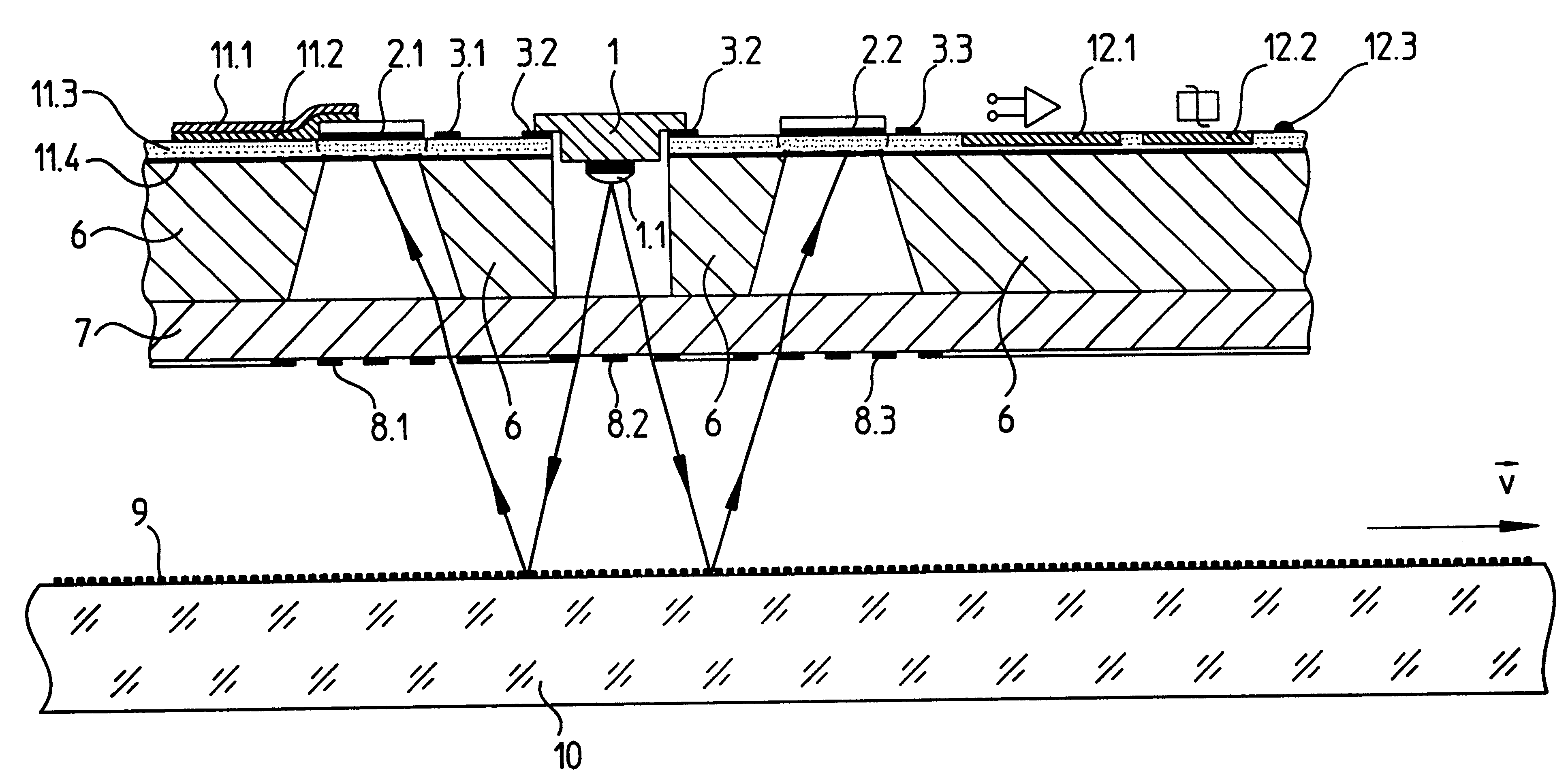
The sensor according to the invention is described below with reference to an exemplary embodiment that contains a length-measuring system. However, it is possible to use the sensor according to the invention in an angle-measuring system, or in a two-dimensional measuring system, without significant modifications.

In the drawing, the optoelectronic sensor of the invention is depicted schematically. On the side of semiconductor substrate 6 facing away from scale 10, photo-diodes 2.1 and 2.2 are arranged underneath passivizing layers 11.1, 11.2, which can be made of silicon oxide and / or silicon nitrite. The manner of manufacturing the photo-diodes is described in German Patent Application 196 18 593 A1, and will not be repeated. Photo diodes 2.1 and 2.2 are produced directly on semiconductor substrate 6, which forms the sensor according to the invention. Two photo diodes 2.1 and 2.2 represent at least one functional assembly, which can contain a plurality of photo diodes or a plurality...


PUM


Abstract

Electronic components of an optoelectronic sensor for a measuring system are arranged on the side of a semiconductor substrate that is facing away from a scale. The semiconductor substrate between electronic components and the scale is removed at those locations where the components emit or detect an electromagnetic beam. In this way, it is possible to arrange all of the electrical connections of the components and further electronic assemblies of the measuring system on a first side of the semiconductor substrate, and all optical components of the measuring system on a second side of the semiconductor substrate.

Description

The present invention relates to an integrated optoelectronic sensor of a measuring system for scanning a scale with graduation markings, and to a method for manufacturing such sensor.DESCRIPTION OF RELATED ARTBritish Patent 1,504,691 and a corresponding German Patent Application 25 11 350 A1 describe a measuring system in which the movement of a first assembly relative to a second assembly is detected. For this purpose, there are two gratings, which are at a constant distance from each other, each being attached to one assembly, When the second grating is illuminated by the divergent light of a light source, the first grating generates a periodic image of the second grating. The image is not stationary if there is a relative motion between the two assemblies.Photo detectors are also included, which have a periodic pattern and are fixedly joined to the second assembly. The first grating is a reflecting grating, and the second grating as well as the photo detectors are essentially in...

Claims


Application Information

Patent Timeline
IPC IPC(8): G01D5/26G01D5/347H01L31/167H01L31/16G01D5/30G01B11/00G01D5/38H01L31/12
CPCG01D5/34715H01L31/167
Inventor SPECKBACHER, PETERMICHEL, DIETER
Owner DR JOHANNES HEIDENHAIN GMBH
Learn More