Gas inlets for wafer processing chamber

a technology of gas inlets and wafers, which is applied in the direction of coatings, metallic material coating processes, chemical vapor deposition coatings, etc., can solve the problems of non-uniform dopant incorporation, no control of dopant gas flow, and temperature dependence of dopant incorporation

Inactive Publication Date: 2002-12-31
APPLIED MATERIALS INC
View PDF34 Cites 53 Cited by
  • Summary
  • Abstract
  • Description
  • Claims
  • Application Information

AI Technical Summary

Benefits of technology

Briefly, this invention provides for a system for supplying processing fluid to a substrate processing apparatus having walls, the inner surfaces of which define a processing chamber in which a substrate supporting susceptor is located. The system consists of a number of fluid storages, each of which stores a separate processing fluid; at least two fluid conduits along which processing fluid flows from the fluid storages to the processing apparatus; and a fluid inlet which connects the fluid conduits to the processing chamber. The inlet has a separate fluid passage, corresponding to each of the fluid conduits, formed along it. Each fluid passage opens at or near an inner surface of a wall to together define a fluid mixing zone, so that fluid moving along one fluid passage is prevented from mixing with fluid moving along any other passage until reaching the mixing zone.

Problems solved by technology

One problem with the doped polysilicon deposition is that the temperature dependence of dopant incorporation is the opposite of the temperature dependence of the polysilicon deposition rate.
This is because adjusting the temperature to obtain thickness uniformity in the polysilicon layer produces a non-uniform dopant incorporation.
There is therefore no control of the dopant gas flow independent of the flow of the silicon species processing gas.
Such deposition is both wasteful and undesirable, as it requires additional cleaning to remove.

Method used


Image

  • Gas inlets for wafer processing chamber
  • Gas inlets for wafer processing chamber
  • Gas inlets for wafer processing chamber

Examples


Embodiment Construction

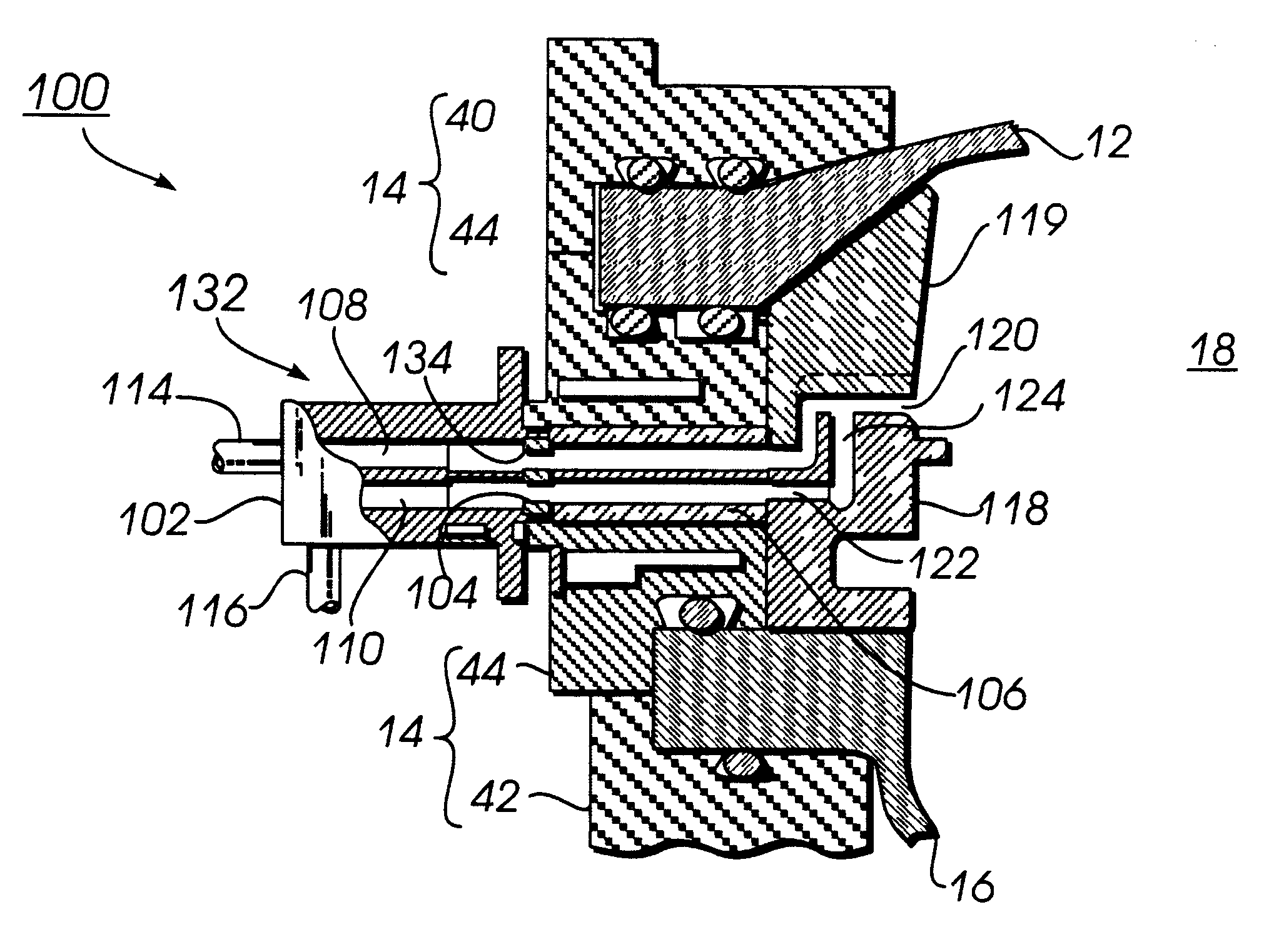
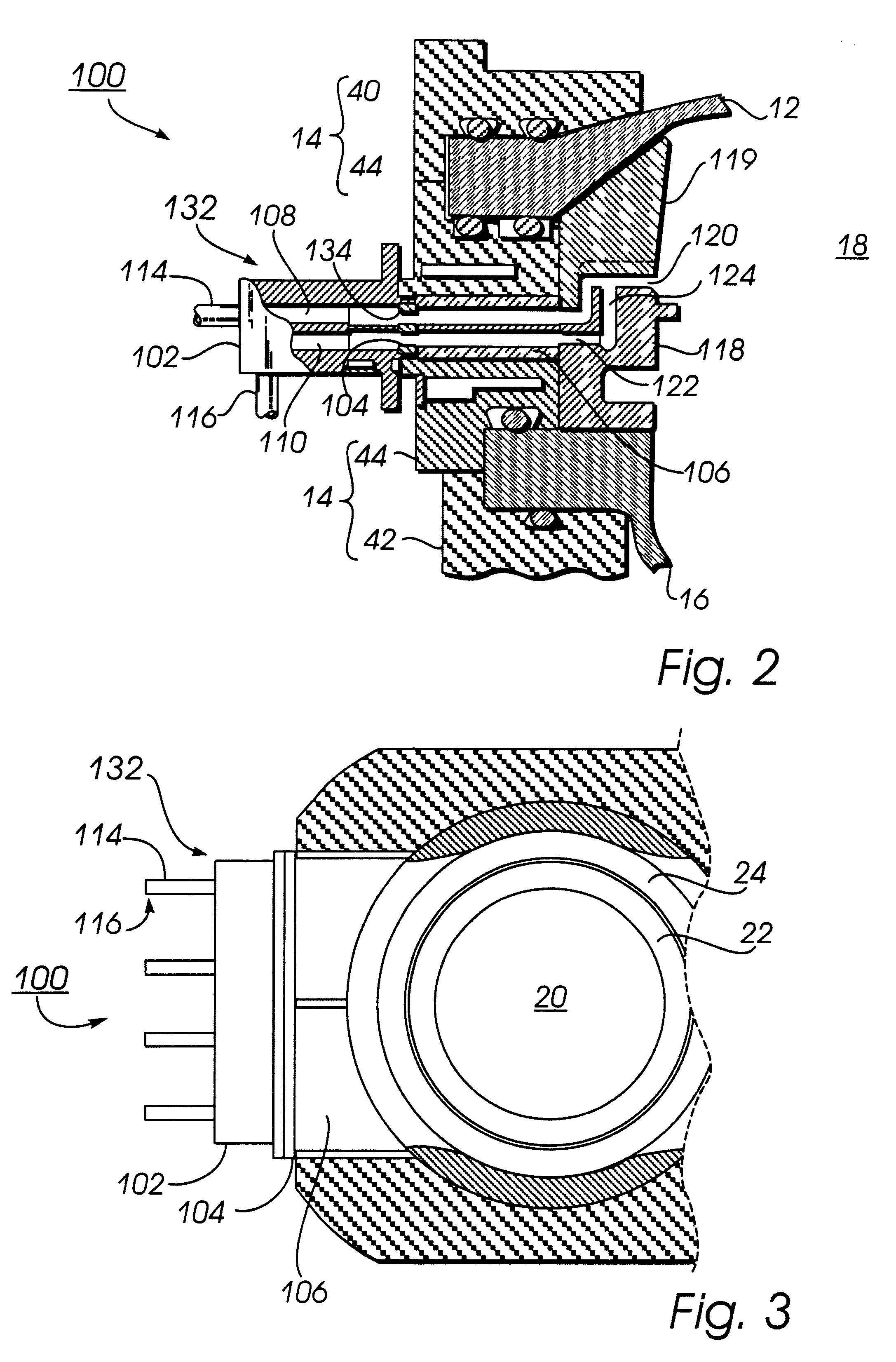
Referring jointly to FIGS. 2, 3 and 4, the improved gas inlet manifold, generally indicated as 100 of the invention, can be seen. The manifold 100 is shown in FIGS. 2 and 3 as connected to the side wall 14 (constituted by upper and lower clamp rings 40, 42 and a base ring 44) of a semiconductor processing apparatus 18.

In all three of these figures, the manifold 100 is shown to include a connector cap 102, a diffuser plate 104 and an interface 106. The connector cap 102 and the interface 106 have upper and lower fluid passages 108 and 110 formed therein. As is apparent from FIG. 4, these upper and lower fluid passageways are oblate in cross section. The diffuser plate 104 has an upper and a lower row of circular holes 112 formed therein. When the diffuser plate 104 is in position between the connector cap 102 and the interface 106, the upper and lower rows of holes 112 correspond respectively to the upper and lower fluid passages 108 and 110. The function of these holes will be descr...


PUM

PropertyMeasurementUnit
areaaaaaaaaaaa
flow rateaaaaaaaaaa
timeaaaaaaaaaa

Abstract

A system for supplying processing fluid to a substrate processing apparatus having walls, the inner surfaces of which define a processing chamber in which a substrate supporting susceptor is located. The system consists of a number of fluid storages, each which stores a separate processing fluid, at least two fluid conduits along which processing fluid flows from the fluid storages to the processing apparatus and a fluid inlet which connects the fluid conduits to the processing chamber. The inlet has a separate fluid passage, corresponding to each of the fluid conduits, formed along it. Each fluid passage opens at or near an inner surface of a wall to define a fluid mixing zone, so that fluid moving along one fluid passage is prevented from mixing with fluid moving along any other passage until reaching the mixing zone.

Description

1. Field of the InventionThis invention relates to semiconductor processing apparatus and, more particularly, to a method and apparatus of supplying two different processing gases to a semiconductor wafer processing chamber.2. Brief Description of the Prior ArtPresent-day equipment for the semiconductor industry is moving toward single substrate processing because processing chambers can be made smaller and processing can be better controlled. Further, modern semiconductor vacuum processing systems have been developed to carry out more than one processing step on a substrate without removing the substrate from a vacuum environment. The use of such vacuum systems results in a reduced number of particulates that contaminate the surface of the wafer during processing, thereby improving the device yield.A typical example of a modern CVD processing apparatus is shown in FIG. 1. In this figure, a single substrate reactor 10 is shown to include a top 12, side walls 14 and a lower portion 1...

Claims


Application Information

Patent Timeline
Patent Type & Authority Patents(United States)
IPC IPC(8): C23C16/455H01L21/00C23C16/44
CPCC23C16/45504C23C16/45512C23C16/45574H01L21/67017H01L21/67023
Inventor ANDERSON, ROGER N.HEY, PETER W.CARLSON, DAVID K.VENKATESAN, MAHALINGAMRILEY, NORMA
Owner APPLIED MATERIALS INC
Why Eureka
Try Eureka