Integrated circuit having a balanced twist for differential signal lines

a technology of integrated circuits and signal lines, which is applied in the direction of digital storage, semiconductor/solid-state device details, instruments, etc., can solve the problems of reducing performance, affecting the performance of pairs, and increasing the voltage differential of bit line pairs

Inactive Publication Date: 2003-01-07
NORTH STAR INNOVATIONS
View PDF12 Cites 35 Cited by
  • Summary
  • Abstract
  • Description
  • Claims
  • Application Information

AI Technical Summary

Benefits of technology

FIG. 1 illustrates a prior art layout in which the routings of a differential pair of signal lines are twisted. A first routing 1 of the differential pair carries signal BL (bit line). The second routing 2 carries signal BLB (bit line bar), and is shunted to a first metal layer 4 with vias 3. As can be seen, only the second routing 2 is in contact with the vias 3, and is shunted to lower metal layer 4. The presence of vias 3 and the lower metal layer 4 induces additional resistance in the signal path of BLB that is not present in the signal path of BL. Also, because a portion of BLB is in a lower metal layer and closer to the active circuitry of the integrated circuit, a capacitive coupling between BLB and the underlying substrate that is greater than the capacitive coupling between BL and the underlying substrate. This asymmetrical configuration may result in resistive and capacitive imbalances in the differential pair, and may also result in signal degradation, reduced signal separation, and higher access times.

Problems solved by technology

As a result, the voltage differential on the bit line pairs is becoming increasingly low.
A problem arises wherein these differential pairs experience crosstalk due to the sidewall coupling with adjacent differential pairs and with the underlying substrate.
This crosstalk results in decreased performance, degradation in signal separation, and reduction in speed.
A problem with the traditional approach of twisting metal routings, however, is that in each twist, one signal transitions between multiple layers of metal while the other does not.
These transitions cause resistive and capacitive imbalances in the differential pair, which may also result in signal degradation and reduced signal separation.
This solution is not suitable to many applications such as memory devices, however, since many bit cells will be followed by an odd number of twists, resulting in asymmetry and many of the same problems associated with a single traditional twist.

Method used


Image

  • Integrated circuit having a balanced twist for differential signal lines
  • Integrated circuit having a balanced twist for differential signal lines
  • Integrated circuit having a balanced twist for differential signal lines

Examples


Embodiment Construction

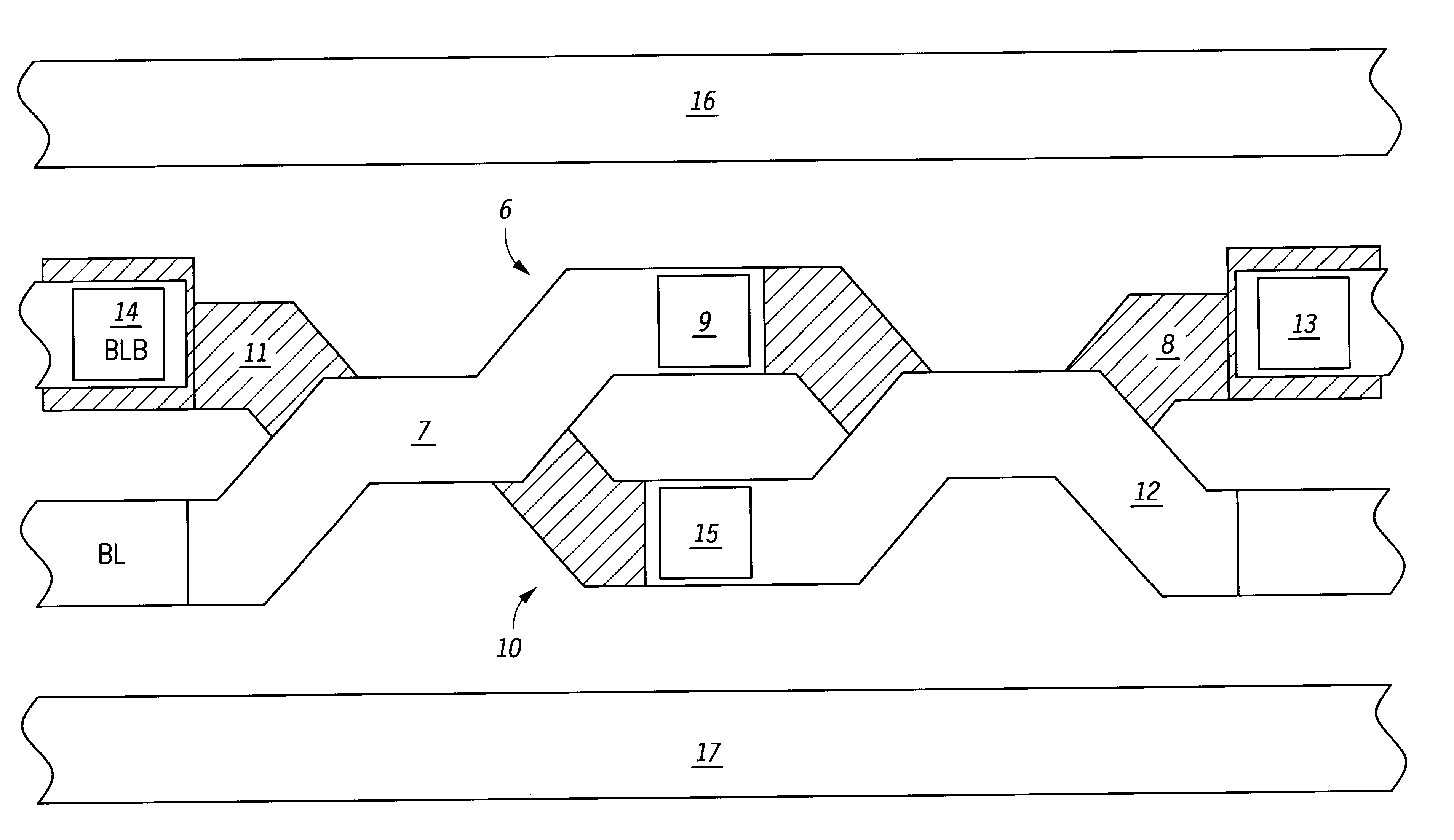
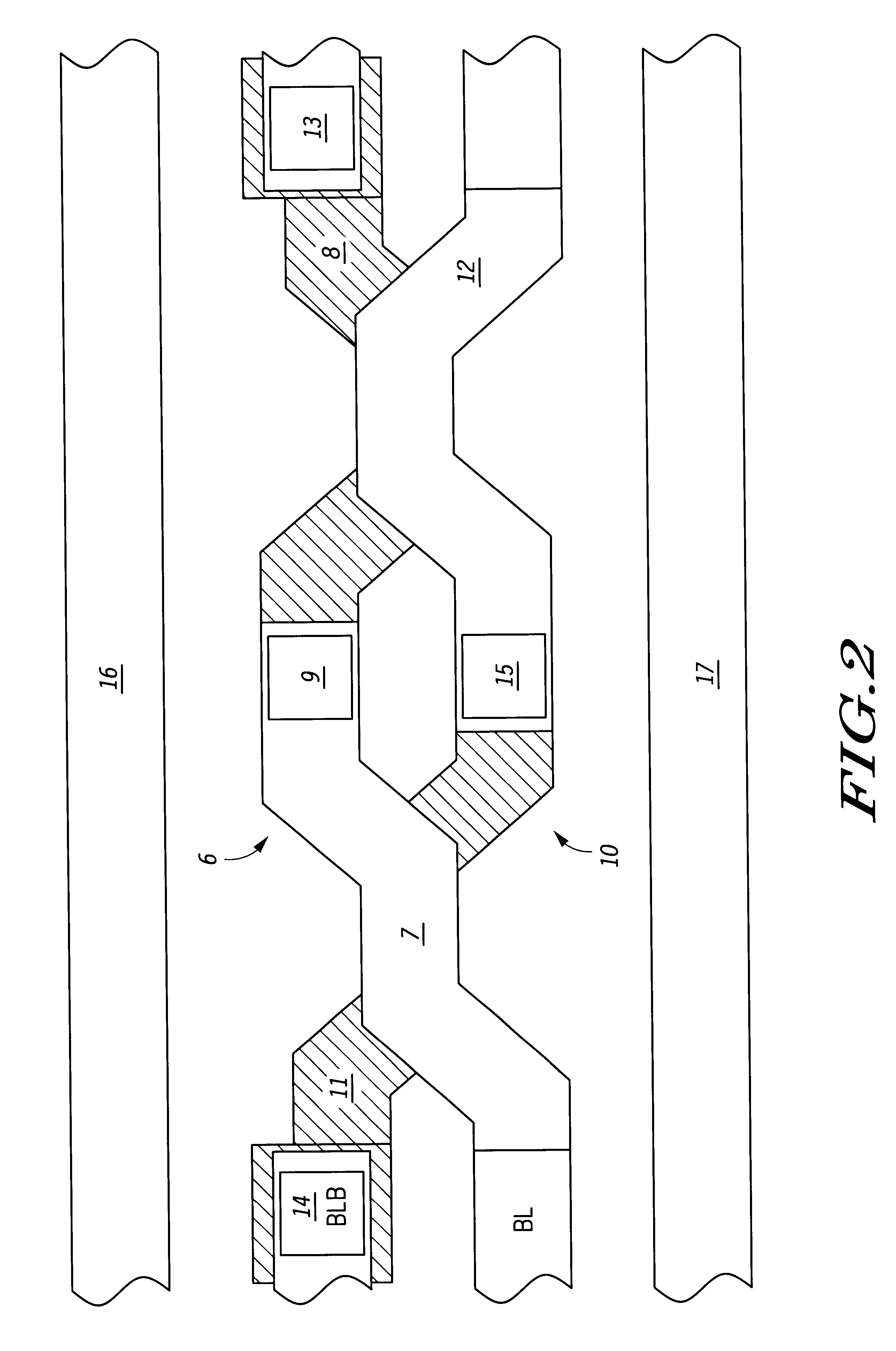
Generally, the present invention provides for twisting differential pairs to reduce the effects of capacitive coupling and to equalize, or balance, the resistance of the differential pairs. The present invention provides a twist configuration that is balanced in terms of resistance, capacitance, and process variance. In the twist design of one embodiment of the present invention, each routing, or line, in the area of the twist passes through both layers of metal. In addition, each routing passes through the same number of vias, and may experience the same number of bends. Each routing will be exposed to the same sidewall crosstalk with adjacent lines since the length of each routing along each sidewall in the same plane is approximately the same. In some embodiments, twisting differential pairs as disclosed herein reduces signal degradation, enhances signal separation, and thus allows a higher clock speed for the integrated circuit.

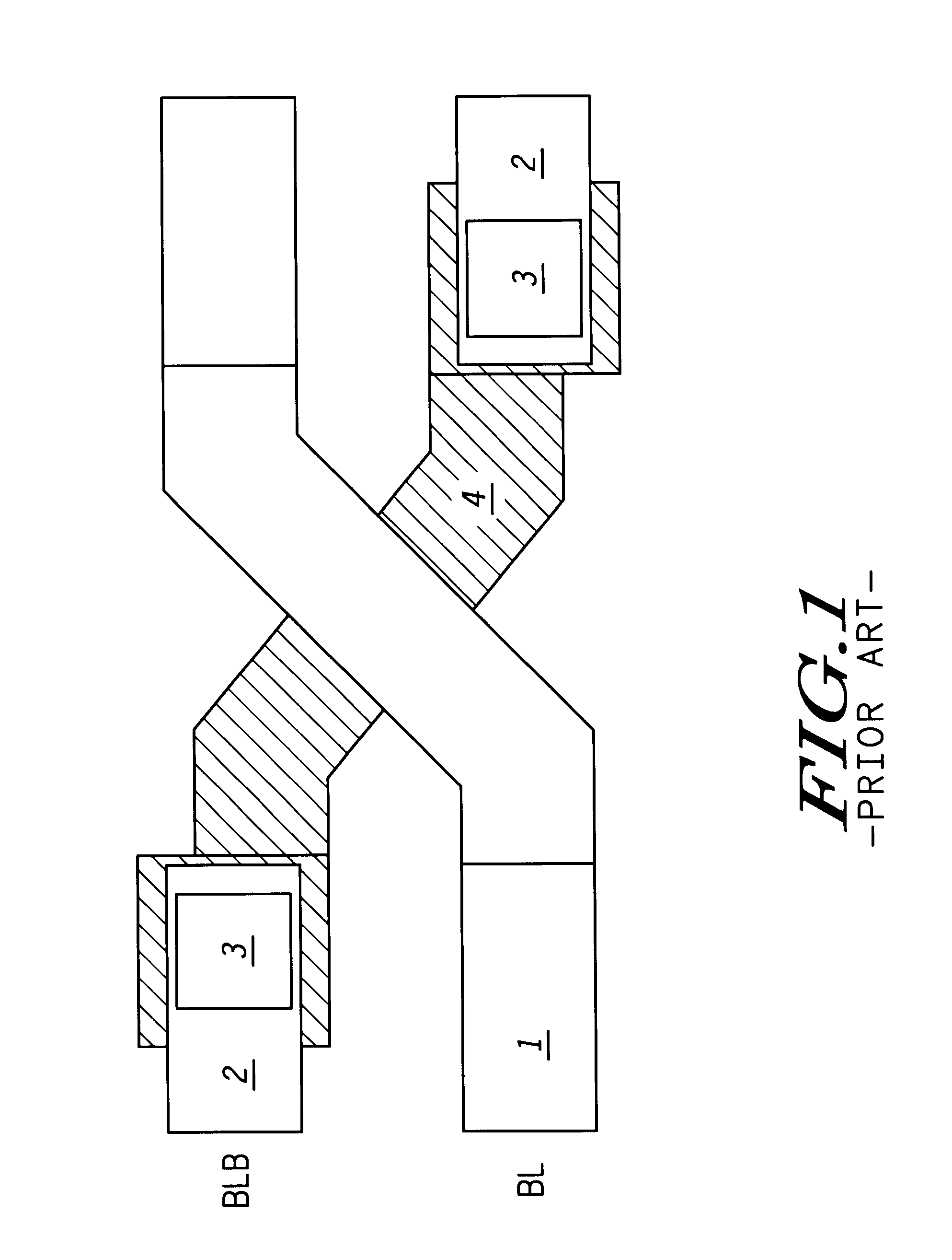
FIG. 1 illustrates a prior art layout in which the ...


PUM


Abstract

A balanced twist design for differential small signal pairs which is balanced in terms of resistance, capacitance and process variance. In the twist design of the present invention, each routing (6, 10) passes through two layers of metal. In addition, each routing (6, 10) passes through the same number of vias (9, 13, 14, 15), and experiences the same number of bends. Each routing (6, 10) is also exposed to the same sidewall crosstalk since the length and width of each routing (6, 10) in both metal layers is approximately the same. As a result, the new twist design reduces signal degradation, enhances signal separation, and allows increased clock speed of the integrated circuit.

Description

This invention relates generally to integrated circuits, and more particularly to balancing differential signal lines in integrated circuits.RELATED ARTIntegrated circuit static random access memories (SRAMs) are used in a variety of applications today. In particular, high speed synchronous SRAMs are used in such applications as caches for computer systems, workstations, and the like. These cache memories provide a high-speed storage of data or instructions that are likely to be reused. As integrated circuit technology,has improved, microprocessors have correspondingly increased in speed. As microprocessor speed increases, the access time of the SRAMs must decrease to provide efficient cache storage.The supply voltage of SRAMs to is being lowered to reduce energy consumption and the generation of heat. For example, some SRAMs operate with a supply voltage of about 1.8 volts. As a result, the voltage differential on the bit line pairs is becoming increasingly low. The importance of s...

Claims


Application Information

Patent Timeline
Patent Type & Authority Patents(United States)
IPC IPC(8): H01L23/522H01L23/52H01L21/82G11C11/413H01L21/8244H01L27/10H01L27/11
CPCH01L23/5225H01L2924/0002H01L2924/00G11C11/413
Inventor ROTH, ALAN S.BANEY, JON D.
Owner NORTH STAR INNOVATIONS
Why Eureka
Try Eureka