Semiconductor device with dummy wiring layers

a technology of semiconductor devices and wiring layers, which is applied in the direction of semiconductor devices, semiconductor/solid-state device details, electrical apparatus, etc., can solve the problem of large amount of dishing at the dummy wiring section

Inactive Publication Date: 2003-01-07
SEIKO EPSON CORP
View PDF9 Cites 30 Cited by
  • Summary
  • Abstract
  • Description
  • Claims
  • Application Information

AI Technical Summary

Benefits of technology

In accordance with one embodiment of the present invention, at least one of the dummy wiring sections has a through hole. In one embodiment, the dummy wiring sections have a plurality of through holes. As a result, a plan area of the dummy wiring sections that overlap device elements formed on a level below the dummy wiring sections is reduced compared to the case where the dummy wiring sections do not have through holes. As a result, observation of the devices formed on the level below the dummy wiring sections by an optical microscope is facilitated.
When the plan configuration of each of the dummy wiring sections is hexagonal, the dummy wiring sections can be disposed highly densely. Also, when the dielectric layer is polished by the CMP method, the dummy wiring sections are strong against circular movements of the polishing cloth. In other words, the dummy wiring sections can more securely absorb polishing pressures applied in many different directions.

Problems solved by technology

In the case of damascene wirings, when the width of the peripheral section of the dummy wiring section exceeds 2 .mu.m, the amount of dishing at the dummy wiring section tends to become large.

Method used


Image

  • Semiconductor device with dummy wiring layers
  • Semiconductor device with dummy wiring layers
  • Semiconductor device with dummy wiring layers

Examples


Embodiment Construction

Preferred embodiments of the present invention are described below with reference to the accompanying drawings.

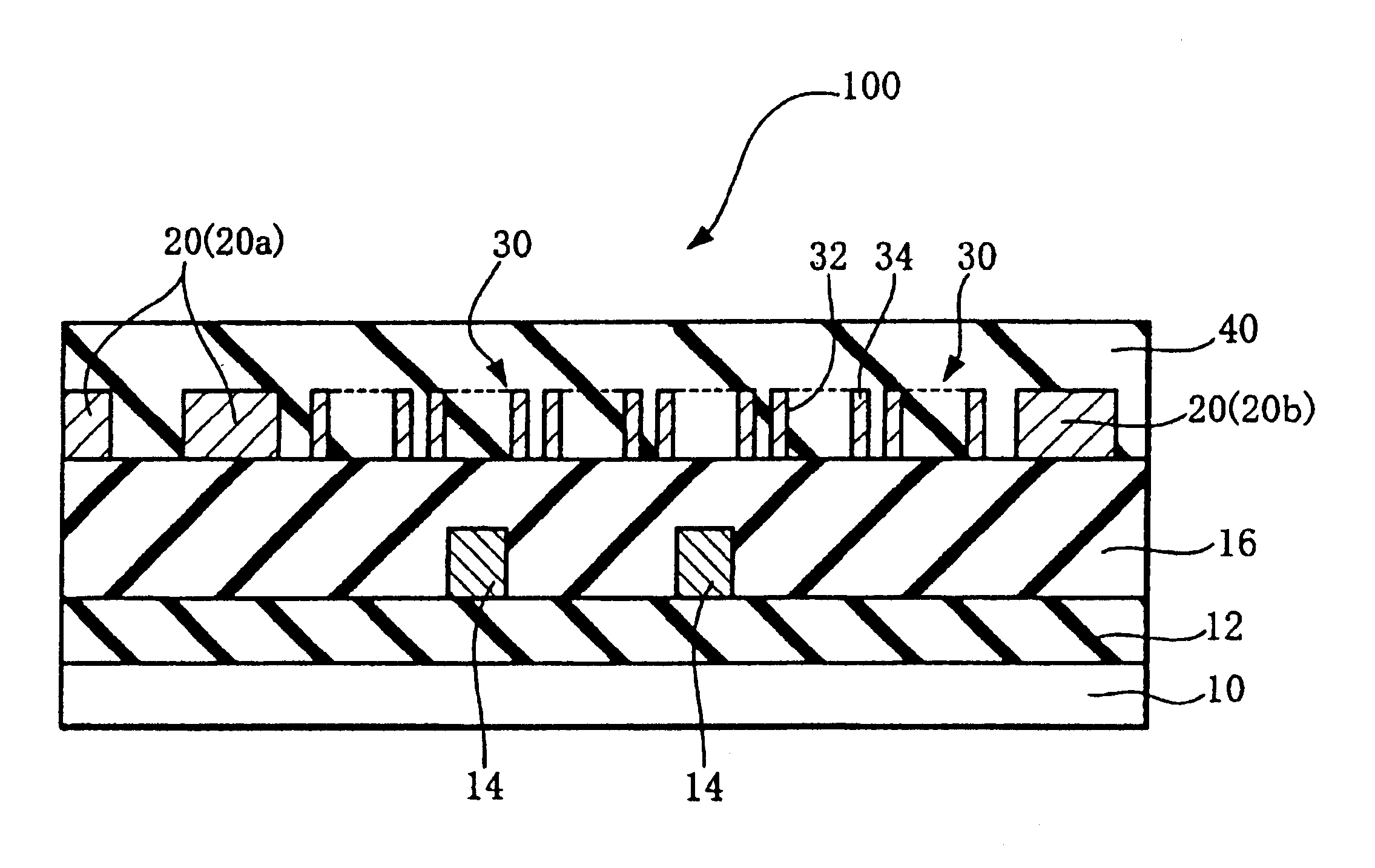
FIG. 1 schematically shows a cross-sectional view of a semiconductor device 100.

The semiconductor device 100 includes a silicon substrate 10. Semiconductor devices (for example, MOSFETs), wiring layers and element isolation regions (not shown) may be formed on a surface of the silicon substrate 10.

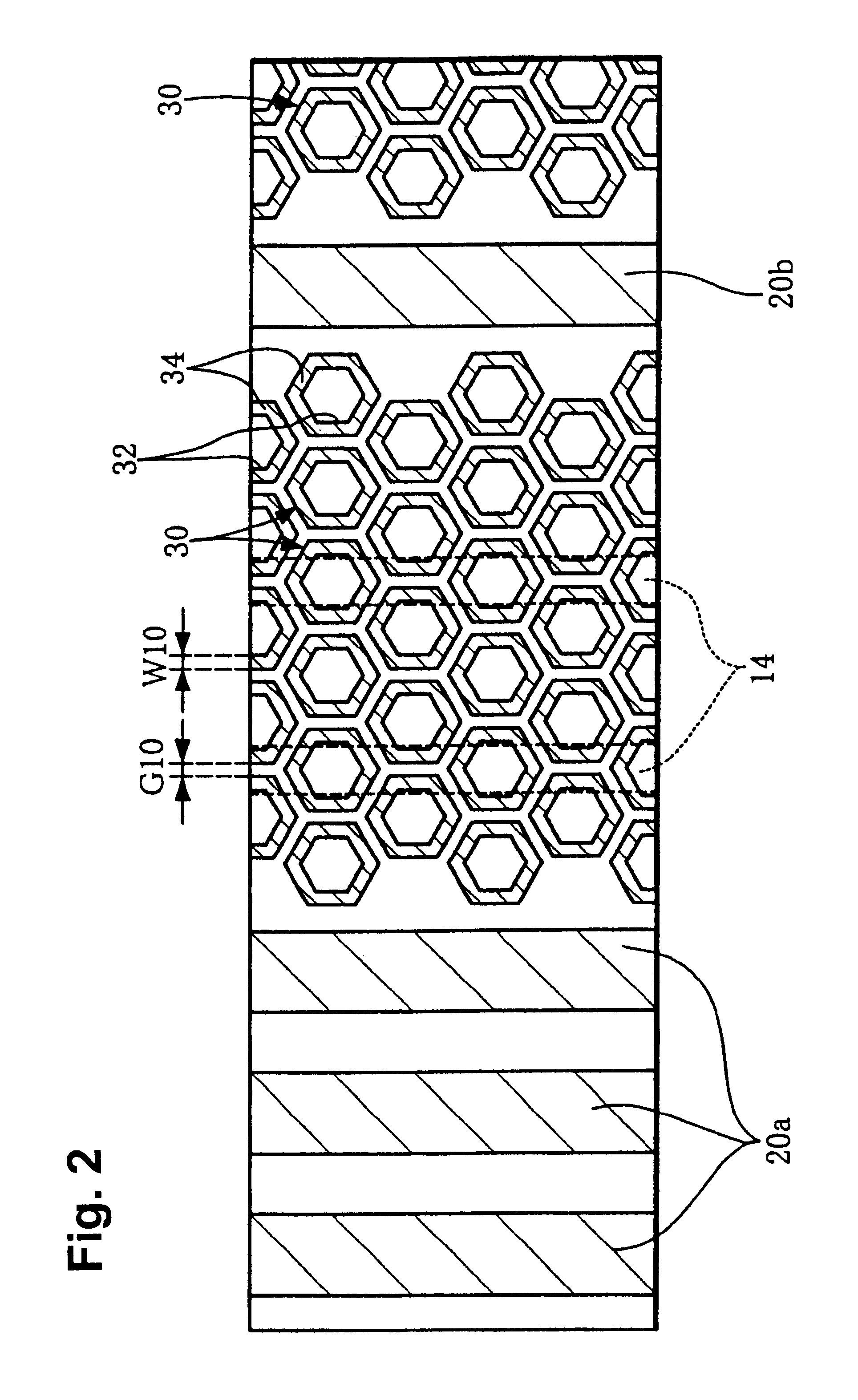
A first interlayer dielectric layer 12, a second interlayer dielectric layer 16 and a third interlayer dielectric layer 40 are successively formed over the silicon substrate 10. A first wiring layer 14 is formed between the first interlayer dielectric layer 12 and the second interlayer dielectric layer 16. A second wiring layer 20 is formed between the second interlayer dielectric layer 16 and the third interlayer dielectric layer 40.

The second wiring layer 20 may include mutually densely formed wiring layers 20a and an isolated wiring layer 20b due to the design of the device. A ...


PUM


Abstract

A semiconductor device 100 has wiring layers 20a and 20b and a plurality dummy wiring sections 30 provided at the same level where the wiring layers 20a and 20b are formed. The dummy wiring sections 30 have at least one through hole 32.

Description

1. Field of the InventionThe present invention relates to a semiconductor device, and more particularly to a semiconductor device having a wiring layer.2. Description of Related ArtPresently, wiring layers are formed in multiple layers in order to accomplish higher integration and further miniaturization of semiconductor devices. Interlayer dielectric layers are formed between wiring layers. The interlayer dielectric layers are planarized by a chemical mechanical polishing method (CMP method).One technique is proposed to improve planarization of the interlayer dielectric layers by the CMP method. In the technique, as shown in FIG. 5, dummy wiring sections 130 are formed between densely formed metal wiring layers 120a and an isolated metal wiring layer 120b on the same level of the metal wiring layers 120a and 120b in the same step in which the metal wiring layers 120a and 120b are formed.However, when the dummy wiring sections 130 are formed, the dummy wiring sections 130 overlap de...

Claims


Application Information

Patent Timeline
Patent Type & Authority Patents(United States)
IPC IPC(8): H01L23/528H01L23/52H01L21/02H01L21/3105H01L21/3205
CPCH01L23/528H01L21/31053H01L2924/0002H01L2924/00
Inventor TAKIZAWA, JUN
Owner SEIKO EPSON CORP
Why Eureka
Try Eureka