
Semiconductor memory device

a memory device and semiconductor technology, applied in the field can solve the problems of high cost, high cost, and high cost of semiconductor memory devices, and achieve the effect of improving the efficiency of timing design, increasing the operating frequency of systems, and increasing the frequency of system operation

Inactive Publication Date: 2003-01-07
RENESAS ELECTRONICS CORP
View PDF11 Cites 29 Cited by
  • Summary
  • Abstract
  • Description
  • Claims
  • Application Information

AI Technical Summary

Problems solved by technology

For example, in recent years the operating frequencies of systems have been increasing, however, the reality is that the performance of semiconductor memory devices has not been keeping pace with the operating speed of systems.
In that sense, it can be said that with conventional synchronous mask ROM, the timing design was very inefficient.
However, there is a problem in that with a synchronous mask ROM like that mentioned above, whatever the CAS latency may be set to, reading can in be performed only at the same operating frequency.
In such a way, with the abovementioned SDRAM also, the timing design is similarly inefficient to the existing synchronous mask ROM.
However, as the operating frequency becomes higher, there is a corresponding reduction in read margin, and hence there is a tendency towards unreliability.

Method used


Image

  • Semiconductor memory device
  • Semiconductor memory device
  • Semiconductor memory device

Examples


Embodiment Construction

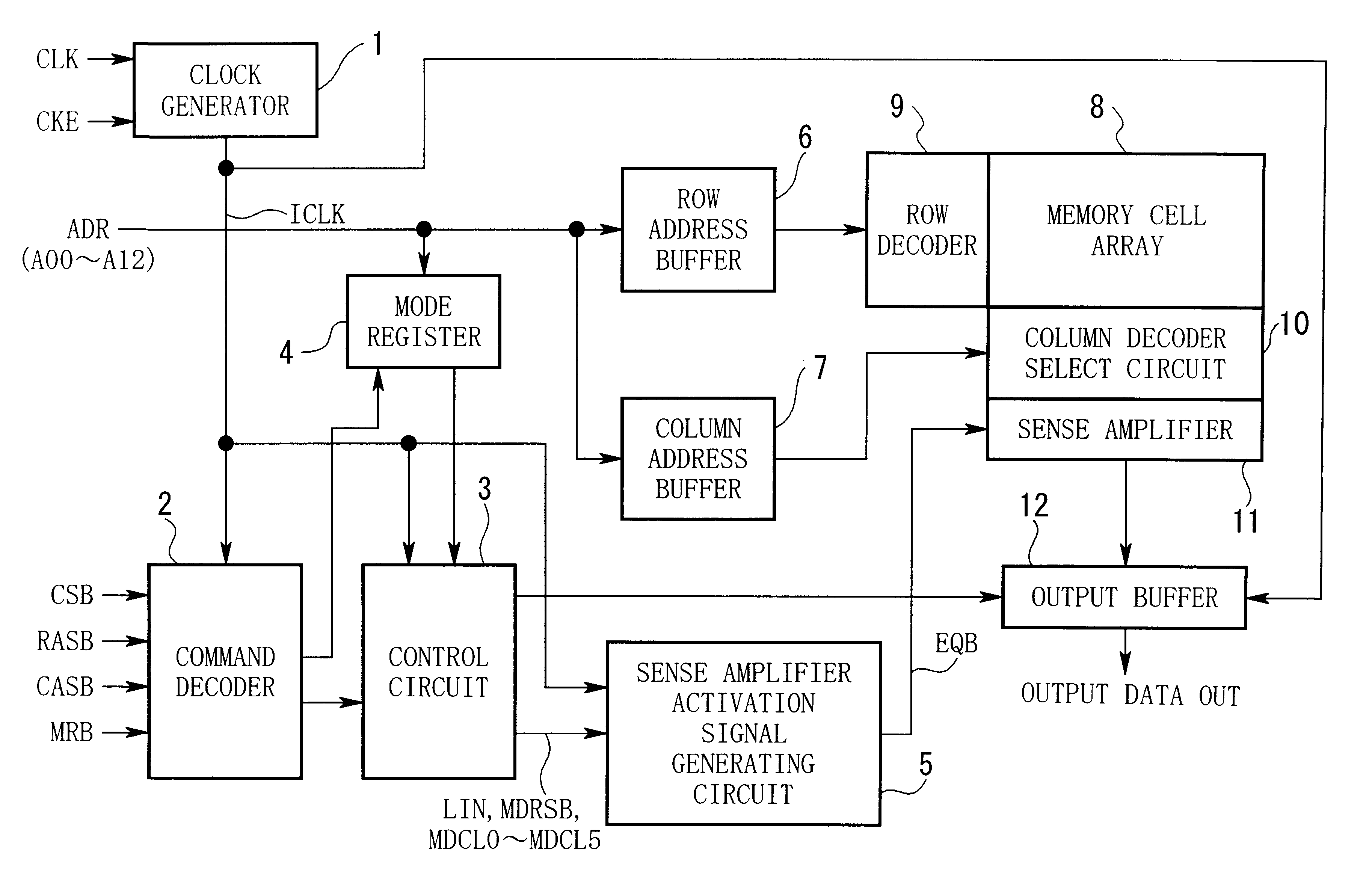
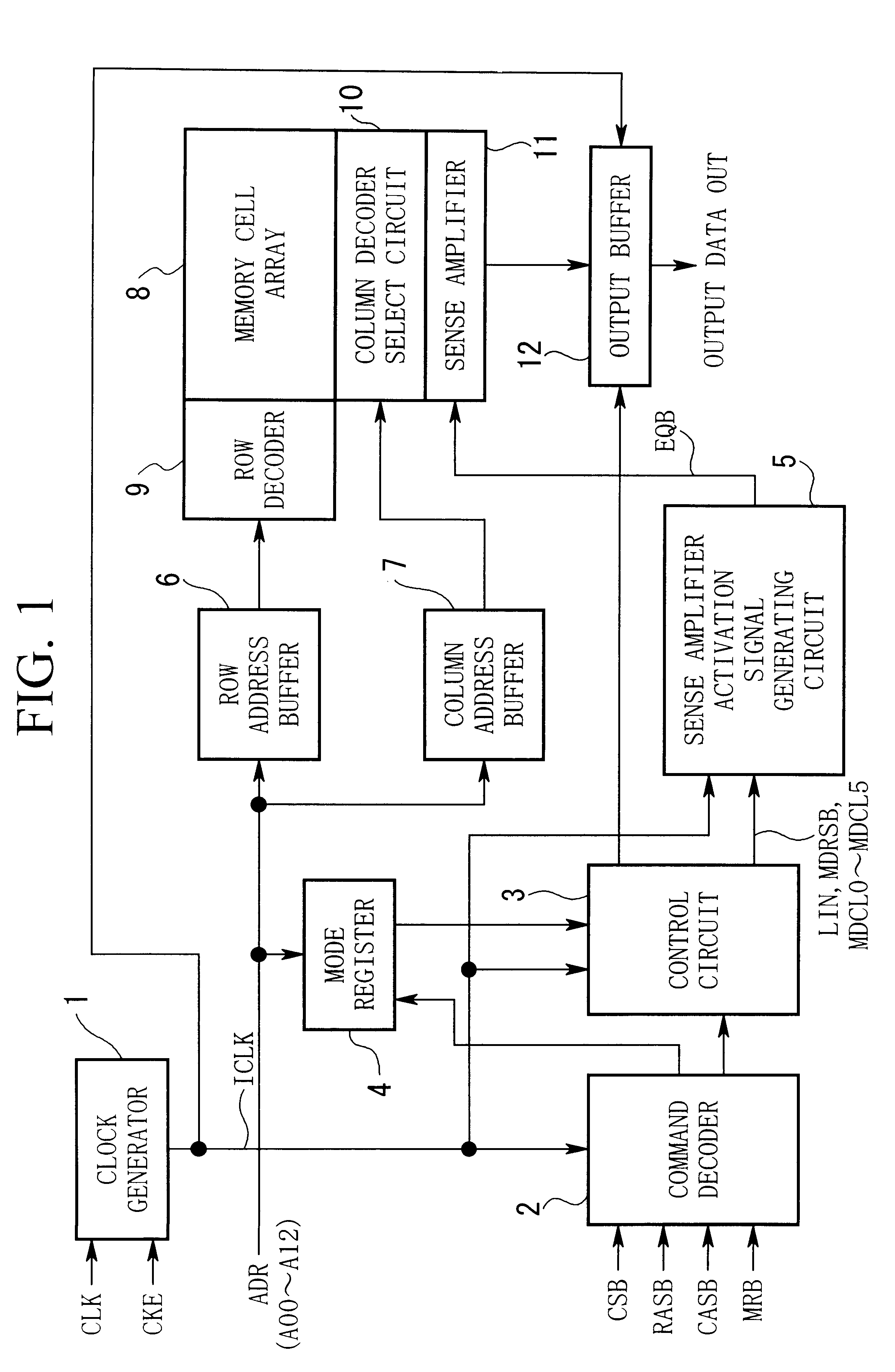
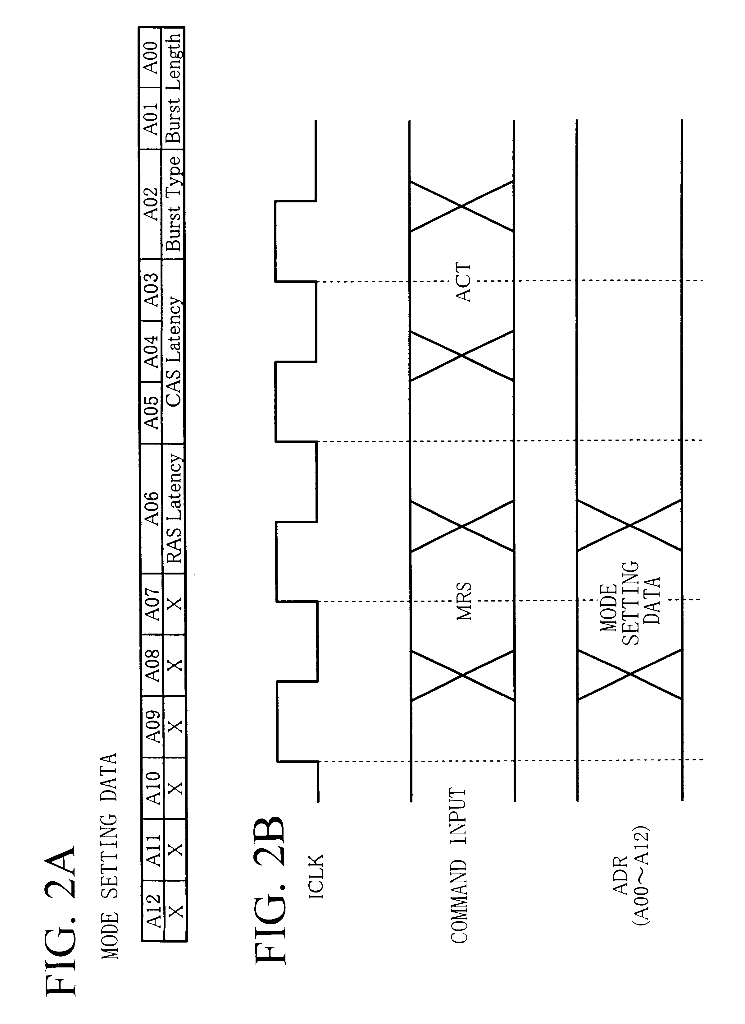
In the abovementioned description, the CAS latency values are "4" through "9". However, this is only one example, and any other number is possible. Furthermore, with the abovementioned description, the arrangement is such that each time CAS latency is increased by "1", the sense amplifier activation period is also extended by one cycle. However, the arrangement does not necessarily need to be like this. For example, the arrangement may be such that, when the CAS latency value is "4" or "5", the width is one cycle for both, and when the CAS latency value is greater than or equal to "6", additional cycles are added as mentioned above. Moreover, for example, the arrangement may be such that when the CAS latency value is "4", the width is one cycle, when the CAS latency value is "5" or "6", the width is two cycles for both, and when the CAS latency value is greater than or equal to "7", additional cycles are added as mentioned above. Moreover, for example, the arrangement may be such th...


PUM


Abstract

To provide a semiconductor memory device that can ensure adequate read margin by effectively utilizing a period for assigned CAS latency. CAS latency is preset before reading. An ACT command is input to activate a word line corresponding to a row address. A READ command is input at a zeroth clock pulse of an internal clock and a digit line corresponding to a column address is connected to a sense amplifier. A sense amplifier activation signal is activated independently of CAS latency to start an equalizing and sense operation. Afterwards, a sense amplifier activation signal is deactivated after two through 5 cycles depending on CAS latency, and the equalizing and sense operation are terminated. Subsequently, an output operation for transferring the sensed result from the sense amplifier to an output pin is performed, and first data is available from a fifth through the eighth clock pulse depending on CAS latency.

Description

1. Field of the InventionThe present invention relates to a semiconductor memory device that is capable of assigning the read time of data stored in memory cells. For example, the invention relates to a semiconductor memory device that controls the read time in terms of latency whose units are defined as the number of cycles of an externally applied clock.2. Description of the Related ArtAmong recent semiconductor memory devices, there is one that can externally assign the read time from the time that the read instruction is given until data stored in a memory cell is read out and is output from the semiconductor memory device. In particular, for synchronous mask ROM (synchronous mask read only memory), SDRAM (synchronous dynamic random access memory) and the like, whose operations are synchronized to the clock of the system that the semiconductor memory devices are used in, a term "latency", which denotes the aforementioned read time by the number of clock cycles, is used.By enabli...

Claims


Application Information

Patent Timeline
Patent Type & Authority Patents(United States)
IPC IPC(8): G11C7/06G11C7/22G11C7/00G11C11/407G11C11/409G11C16/02
CPCG11C7/06G11C7/22G11C2207/2281G11C11/407
Inventor HIRAKAWA, TSUYOSHI
Owner RENESAS ELECTRONICS CORP
Learn More