Semiconductor device and its manufacturing method

a technology of semiconductors and manufacturing methods, applied in the direction of instruments, optics, transistors, etc., can solve the problems of linear defects and increased manufacturing costs

Inactive Publication Date: 2003-01-21
SEMICON ENERGY LAB CO LTD
View PDF18 Cites 81 Cited by
  • Summary
  • Abstract
  • Description
  • Claims
  • Application Information

AI Technical Summary

Problems solved by technology

In particular, in the display unit of a projection type, a problem exists in that one portion of light emitted from the liquid crystal display unit is reflected on the interface of a substrate and an air layer and is also reflected in an optical system, and is returned in a reverse direction a

Method used


Image

  • Semiconductor device and its manufacturing method
  • Semiconductor device and its manufacturing method
  • Semiconductor device and its manufacturing method

Examples


embodiment 1

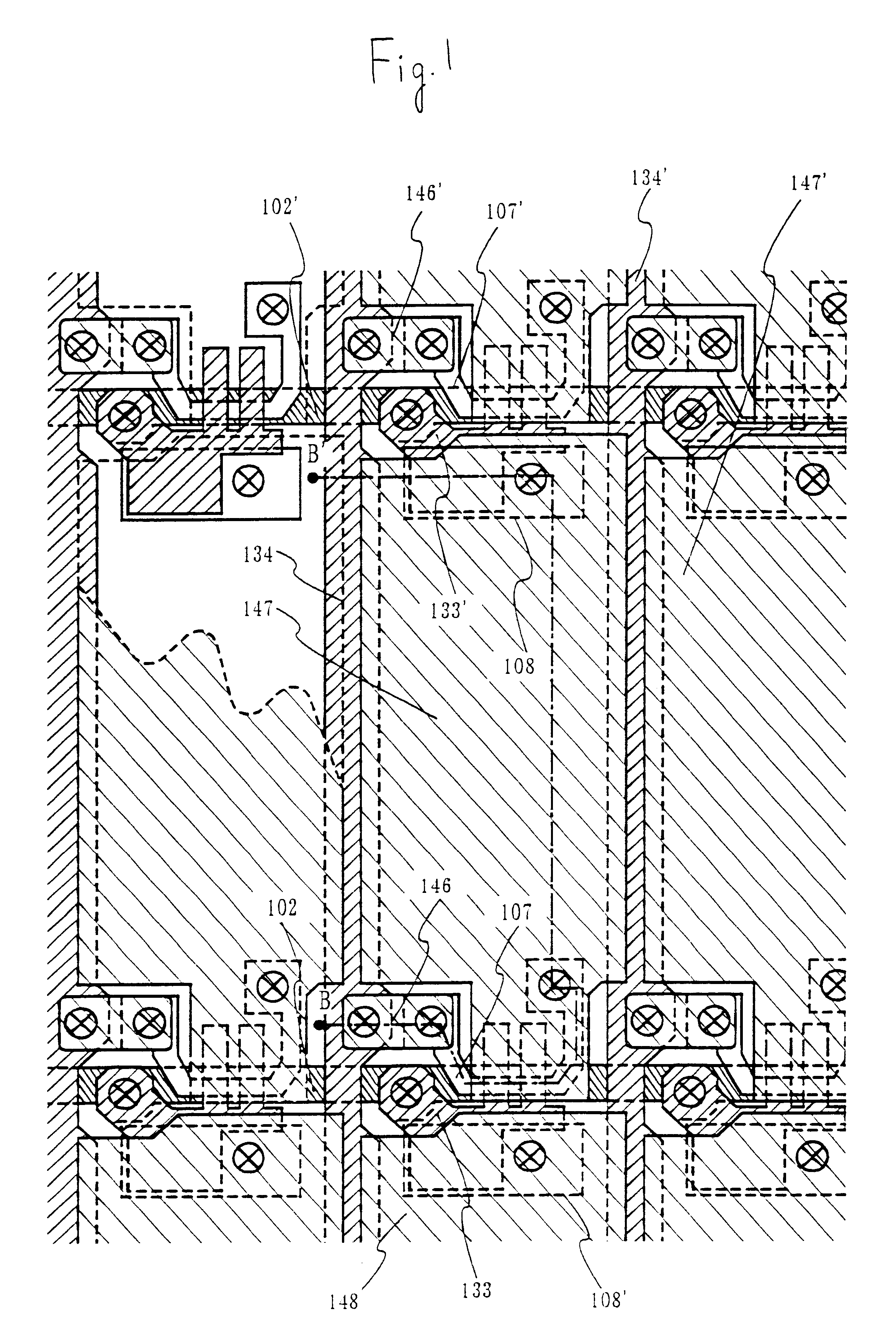
In this embodiment, a forming method of the pixel portion having the structure shown in FIG. 1 will be explained in detail by using the drawings. A process for forming a driving circuit constructed by an n-channel type TFT and a p-channel type TFT will be also explained simultaneously. In this embodiment, the explanations are made by using reference numerals common to FIGS. 1 to 7 for convenience.

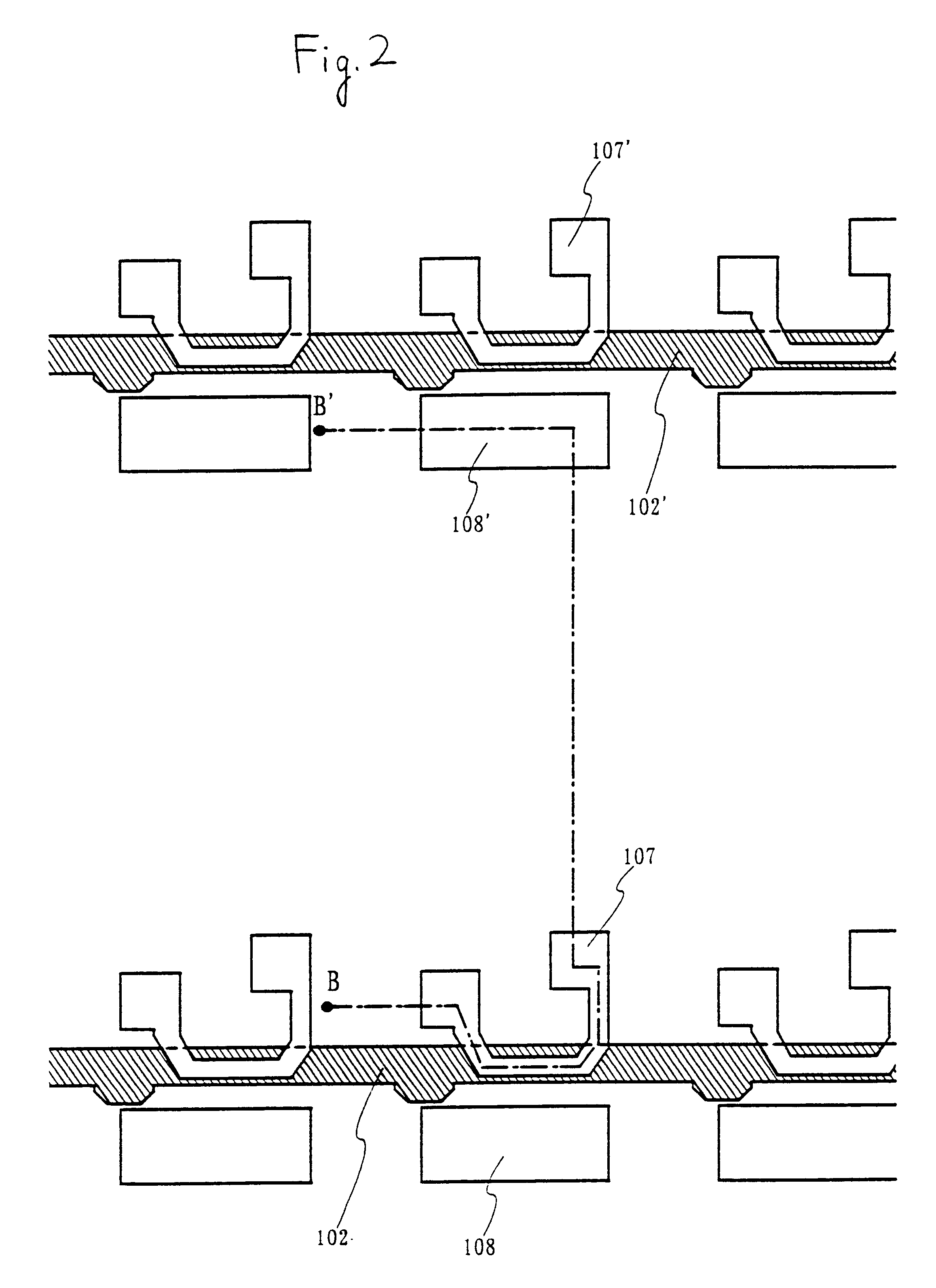
FIGS. 2 and 3 are plan views for explaining a manufacturing process of the pixel structure of the invention. FIG. 4 is a plan view for explaining the manufacturing process of the TFT formed in a driving circuit portion. FIGS. 5 to 7 show longitudinal sectional views corresponding to these plan views.

As shown in FIG. 5A, scanning lines (gate lines) 102, 103 are first formed on a substrate 101. No substrate 101 is particularly limited if this substrate 101 has an insulating surface. The substrate 101 is typically constructed by using a non-alkali glass substrate such as alumino borosilicate g...

embodiment 2

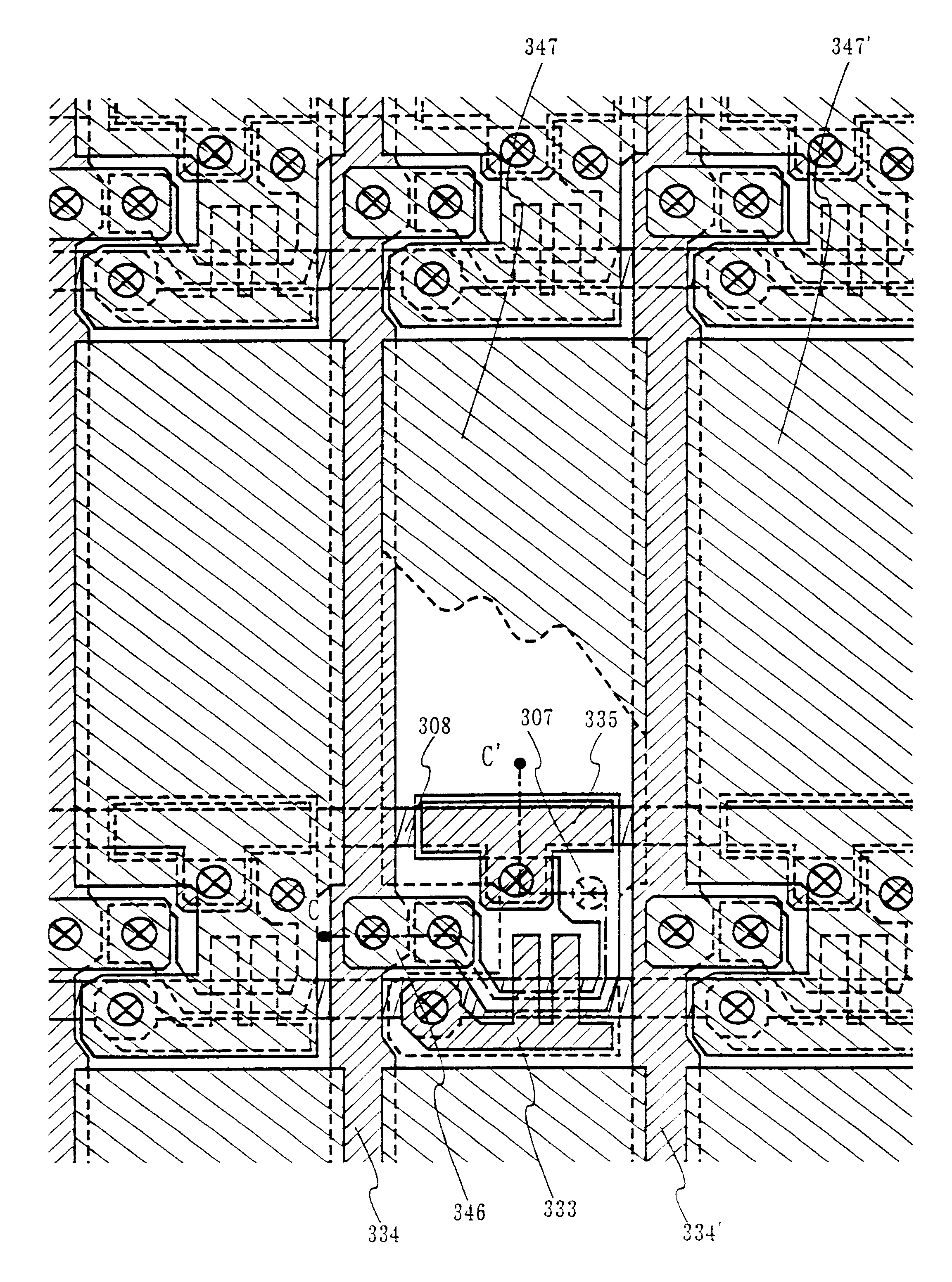
The pixel structure of an accumulating capacity type adopts the same structure as the embodiment 1 except for a difference in the construction of an auxiliary capacity portion. FIG. 8 shows a plan view of this pixel structure of the accumulating capacity type. FIG. 9 shows a cross-sectional view corresponding to a C-C' line of FIG. 8. In this embodiment, an explanation will be made by using reference numerals common to FIGS. 8 and 9 for convenience.

A scanning line (gate line) 303 and a capacity line 308 are formed on a substrate 301 shown in FIG. 9. Semiconductor films 306, 307 are formed on a first insulating layer 304 so as to be partially overlapped with wirings of the scanning line and the capacity line. Further, a second insulating layer 309 functioning as a gate insulating film is formed, and gate electrodes 332 to 333, a data line 334 and a capacity electrode 335 are formed. In an n-channel type TFT 255, the gate electrode and the scanning line (gate line) are connected to ea...

embodiment 3

When the display unit of a transmission type is formed, the pixel electrode is formed by a transparent electroconductive film. FIG. 11 shows a pixel structure when the display unit of the transmission type is formed by using the invention. A pixel electrode 180 is formed by using a transparent electroconductive film such as ITO. Connection with a semiconductor film for forming a TFT and an auxiliary capacity portion is made by connecting electrodes 181 and 182. FIG. 12 shows a cross-sectional view corresponding to a D-D' line. An n-channel type TFT 205 and an auxiliary capacitor 206 are manufactured similarly to the embodiment 1. The pixel electrode 180 is formed after a contact hole is formed in an interlayer insulating film 142. Thereafter, the connecting electrodes 181, 182a reformed by using Ti and Al. The connecting electrode 181 is formed on a channel forming area of a semiconductor film forming the n-channel type TFT 205, and also functions as a light interrupting film simila...


PUM


Abstract

An object of the present invention is to provide an active matrix type display unit having a pixel structure in which a pixel electrode formed in a pixel portion, a scanning line (gate line) and a data line are suitably arranged, and high numerical aperture is realized without increasing the number of masks and the number of processes. In this display unit, a first wiring arranged between a semiconductor film and a substrate through a first insulating film is overlapped with this semiconductor film and is used as a light interrupting film. Further, a second insulating film used as a gate insulating film is formed on the semiconductor film. A gate electrode and a second wiring are formed on the second insulating film. The first and second wirings cross each other through the first and second,insulating films. A third insulating film is formed as an interlayer insulating film on the second wiring, and a pixel electrode is formed on this third insulating film. The pixel electrode can be overlapped with the first and second wirings so that an area of the pixel electrode can be increased in the display unit of a reflection type.

Description

1. Field of the InventionThe present invention relates to a semiconductor device having a pixel portion or having this pixel portion and its driving circuit on the same insulator surface. In particular, the invention can be suitably used in a display unit in which a liquid crystal material is provided between electrodes. In this specification, the semiconductor device generally means a device able to function by utilizing semiconductor characteristics, and the above display device, an integrated circuit and an electronic device mounting the integrated circuit and the display unit thereto belong to a category of the semiconductor device.2. Description of the Related ArtA matrix driving system (this is called an active matrix driving system) for arranging a thin film transistor (hereinafter abbreviated as TFT) every pixel or dot has become an indispensable technique as high definition of pixel density is advanced:. The active matrix driving system using the TFT can prevent crosstalk g...

Claims


Application Information

Patent Timeline
IPC IPC(8): H01L29/66H01L21/336H01L29/786H01L21/02G02F1/13G02F1/1368
CPCH01L29/66757H01L29/78621H01L27/124H01L29/78645H01L29/78648G02F1/1368H01L29/78633
Inventor YAMAZAKI, SHUNPEI
Owner SEMICON ENERGY LAB CO LTD
Why Eureka
Try Eureka