Single structure all-direction ESD protection for integrated circuits

Inactive Publication Date: 2003-01-28
ILLINOIS INSTITUTE OF TECHNOLOGY
View PDF20 Cites 77 Cited by
  • Summary
  • Abstract
  • Description
  • Claims
  • Application Information

AI Technical Summary

Problems solved by technology

ESD events, which are inevitable in integrated circuit (IC) manufacturing, assembly, and application, generate huge over-current and over-voltage pulses that can fatally damage electronic components.
ESD failure emerges as the major reliability concern to the IC industry, accounting for up to thirty percent of field failures.
This

Method used


Image

  • Single structure all-direction ESD protection for integrated circuits
  • Single structure all-direction ESD protection for integrated circuits
  • Single structure all-direction ESD protection for integrated circuits

Examples


Embodiment Construction

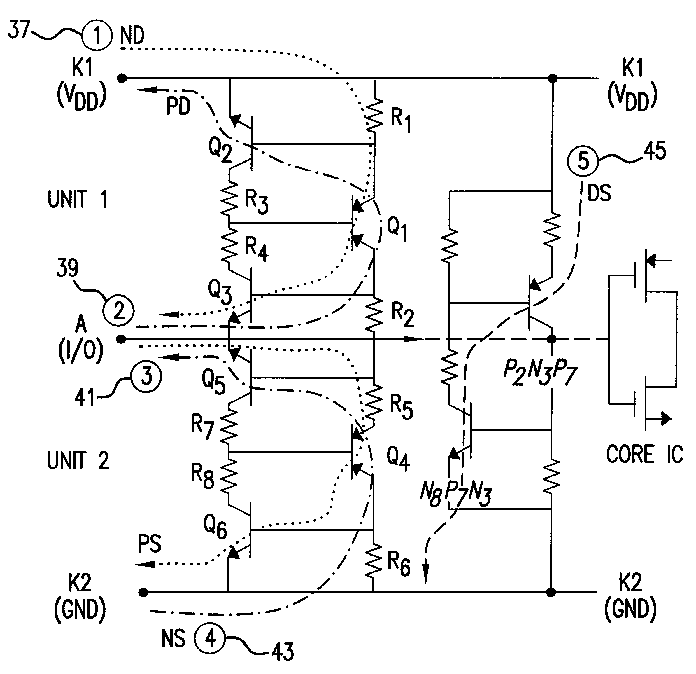
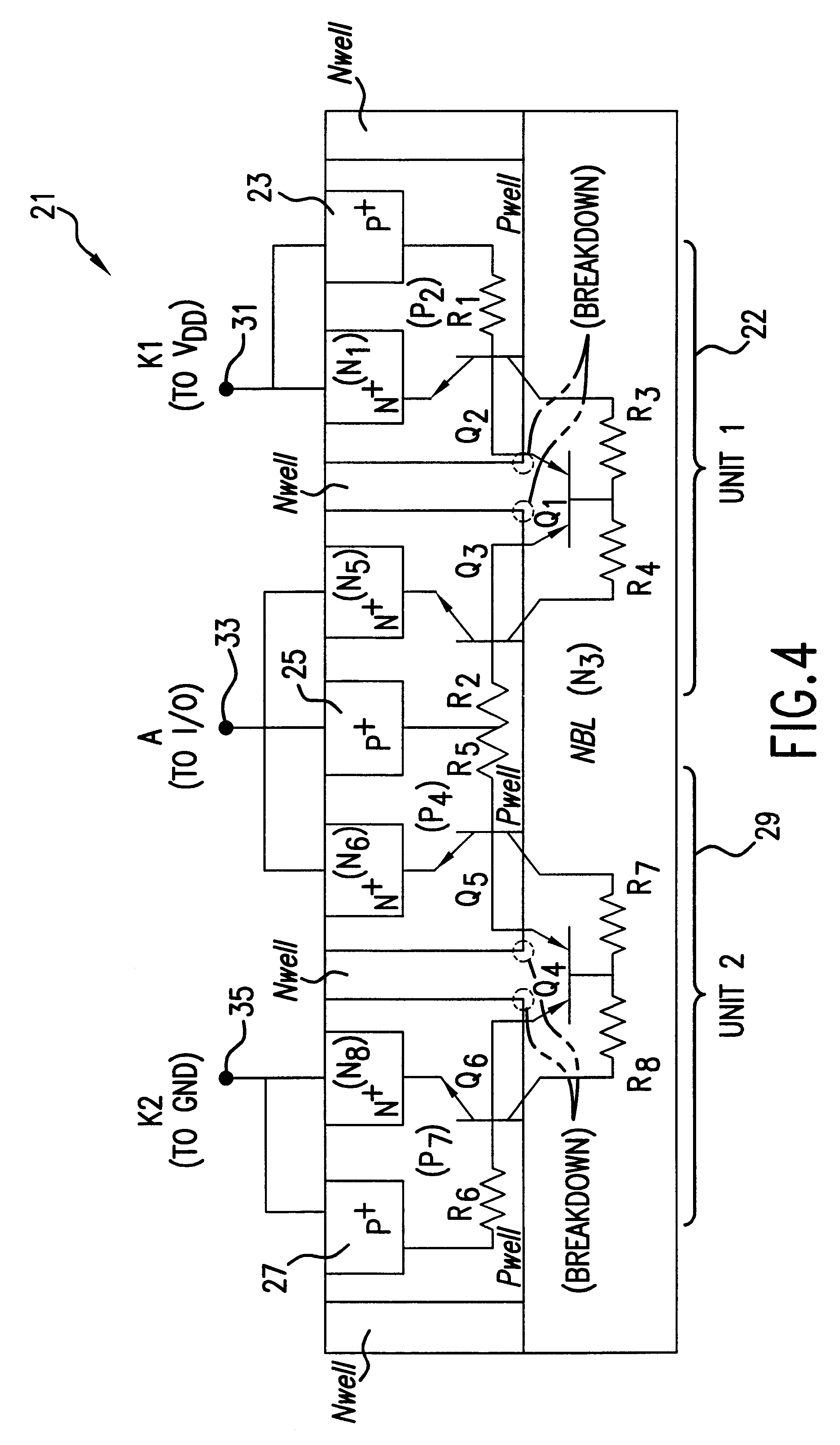
The ESD protection structure 21 seen in cross-section in FIG. 4, has three terminals, namely I / O, V.sub.DD, and GND. The structure has eight layers: N.sub.1, P.sub.2, N.sub.3, P.sub.4, N.sub.5, N.sub.6, P.sub.7, N.sub.8. The intrinsic electronic circuitry structure is added for clarity to FIG. 4.

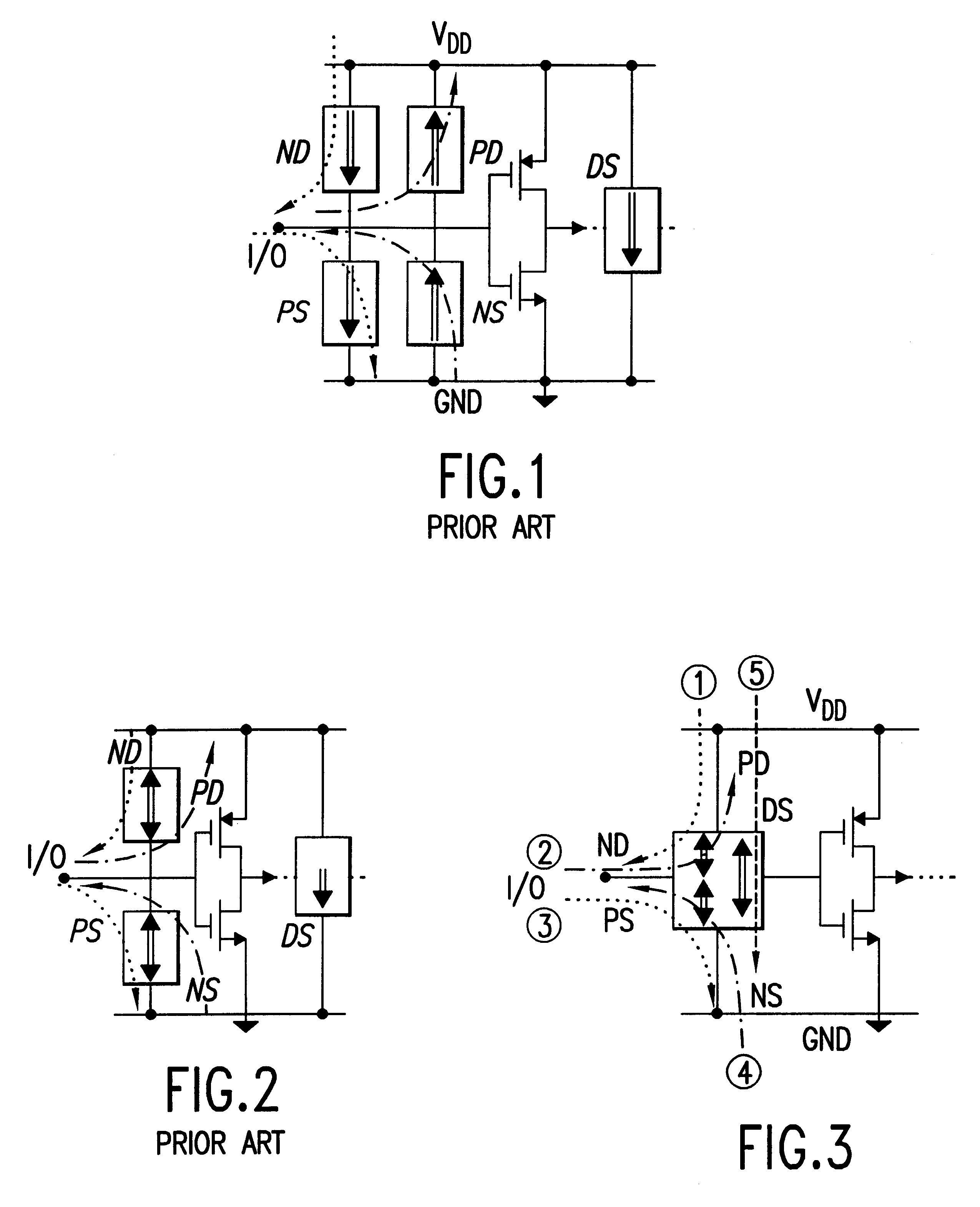
There are three P-type tubs: P.sub.2, P.sub.4 and P.sub.7 ; with each having a P+ contact 23, 25, 27, respectively, and at least one N+ contact N.sub.1 in P.sub.2 ; N.sub.5 and N.sub.6 in P.sub.4 ; and N.sub.8 in P.sub.7. The three P-type tubs P.sub.2, P.sub.4 and P.sub.7 are formed in the N-type well, or N Boundary Layer NBL, N.sub.3. Six bipolar transistors Q.sub.1 -Q.sub.6 and eight parasitic resistors R.sub.1 -R.sub.8 are formed as electrically connected entities and may be grouped into two functional protection subcircuits: upper, or right, unit one and lower, or left, unit two.

The upper protection subcircuit 22 consists of Q.sub.1 -Q.sub.3 and R.sub.1 -R.sub.4. Q.sub.1 is formed by P.s...


PUM


Abstract

An overvoltage/overcurrent electrostatic discharge protection single circuit structure for Integrated Circuits protects on all paths and polarities between In/Out, Supply, and Ground pins. The structure is built on the chip substrate with an N well with three P Diffusions therein each containing N+ and P+ diffusions therein to form 6 transistors and 8 parasitic resistors to yield 5 thyristors. The structure provides very fast, symmetrical, full protection while using minimal chip area.

Description

1. Field of the InventionThe present invention relates to protection for semiconductor integrated circuits from over-voltage and over-current conditions caused by electrostatic discharge (ESD). The present invention relates more specifically to a single structure ESD protection circuit using active devices integrated therein.2. Description of Prior ArtESD events, which are inevitable in integrated circuit (IC) manufacturing, assembly, and application, generate huge over-current and over-voltage pulses that can fatally damage electronic components. ESD failure emerges as the major reliability concern to the IC industry, accounting for up to thirty percent of field failures. Therefore, industrial standards generally require on-chip ESD protection circuits for all IC chips.In general principle, an ESD protection circuit is off, or open in normal operation and is triggered on, or closed, during an ESD event to form a low impedance path to shunt the current surge and to clamp the pin vol...

Claims


Application Information

Patent Timeline
IPC IPC(8): H02H9/00H01L27/02
CPCH01L27/0251
Inventor WANG, ALBERT ZIHUI
Owner ILLINOIS INSTITUTE OF TECHNOLOGY
Why Eureka
Try Eureka