Dual layer hard mask for eDRAM gate etch process

a technology of edram gate etching and hard masking, which is applied in the direction of basic electric elements, electrical equipment, semiconductor devices, etc., can solve the problems of narrow process windows, difficult manufacturing, and higher manufacturing costs of methods

Inactive Publication Date: 2003-02-11
INFINEON TECH AG +1
View PDF5 Cites 14 Cited by
  • Summary
  • Abstract
  • Description
  • Claims
  • Application Information

AI Technical Summary

Problems solved by technology

However, this method has a higher manufacturing cost due to the use of two DUV masks.
The dra...

Method used


Image

  • Dual layer hard mask for eDRAM gate etch process
  • Dual layer hard mask for eDRAM gate etch process
  • Dual layer hard mask for eDRAM gate etch process

Examples


Embodiment Construction

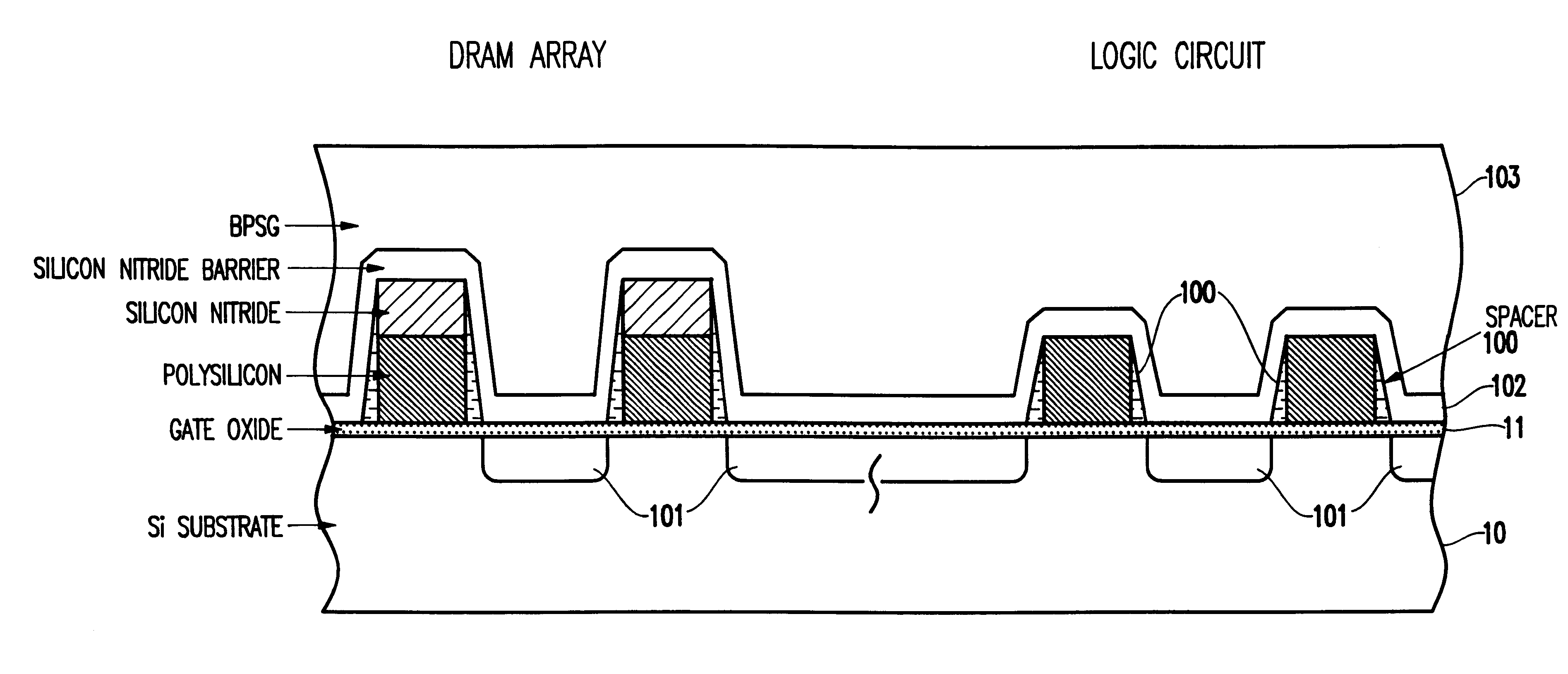
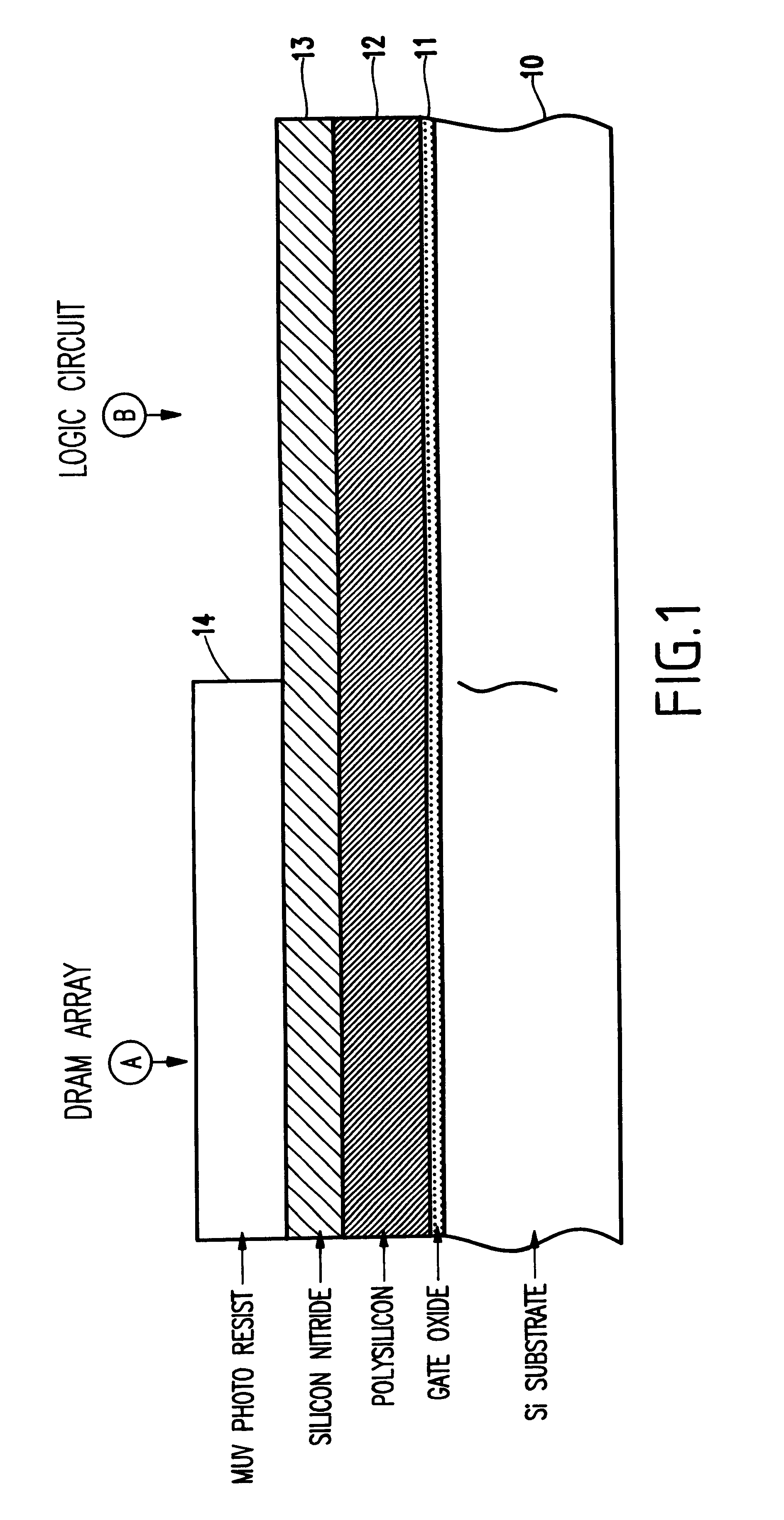
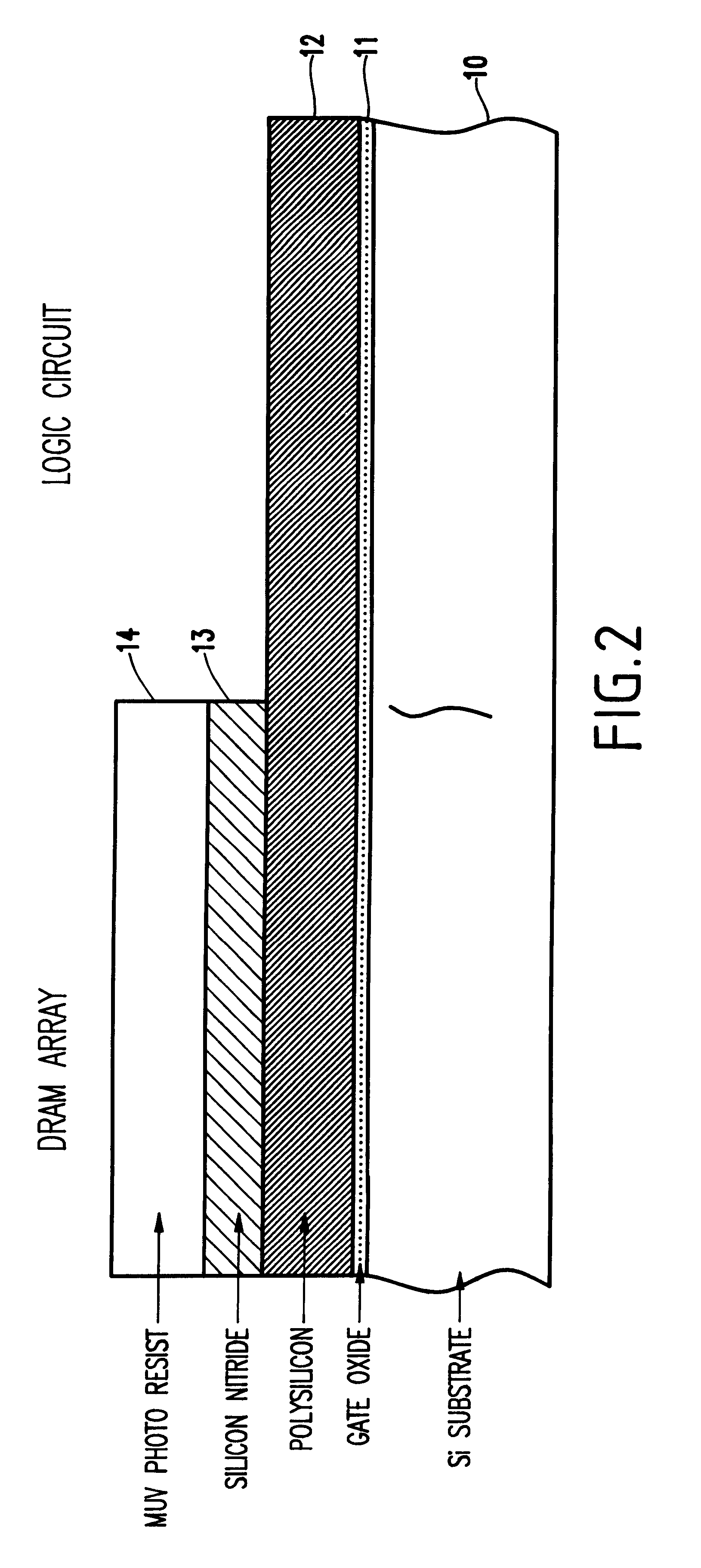
This invention generates self-aligned, borderless contacts in DRAM arrays and bordered contacts in logic support area on eDRAM products using a single contact definition process (lithography and etch). Referring now to the drawings, and more particularly to FIG. 1, this figure shows a simplified cross section of a wafer intended to have an eDRAM array in region A and support logic circuitry in region B. The wafer includes substrate 10 which has been covered by a gate oxide layer 11 and a polysilicon layer 12.

Gate oxide layer 11 and polysilicon layer 12 interplay with the invention since a key aspect of the method is that of allowing regions on the same chip having two different layout styles, where both regions have devices using the oxide layer for transistor gate insulators and the polysilicon layer as gate contacts. This effect is achieved by introducing a thick nitride etch stop layer 13 (approximately 100 nm) which will remain only in the array area A at the hardmask stage, mea...


PUM


Abstract

A method of fabricating an integrated circuit chip having a first region of a first layout rule and a second region of a second layout rule. The method includes using a first material to establish a first hard mask pattern in only the first region and using a second material to establish a second hard mask pattern on top of the first hard mask pattern. The second material is additionally used to establish a third hard mask pattern in the second region.

Description

1. Field of the InventionThis invention relates generally to the fabrication of integrated circuit devices. The invention particularly relates to integrating, on a single chip of "embedded Dynamic Access Memory" (eDRAM) products, self-aligned, borderless contacts in DRAM arrays in a first region and bordered contacts in a logic support area in a second region, using a single poly-Si patterning process (lithography and etch) and a single contact definition process. The invention addresses the problem of fabrication of an integrated circuit chip having two different layout rules on the same chip. In this case, a highly packed layout is used for the gate contacts of the DRAM array region in contrast to a more separated layout for gate contacts in the region containing support logic circuits. Components are concurrently fabricated in both areas, overcoming prior art techniques of having to deal separately with the respective region devices.2. Description of the Related ArtIn a prior fil...

Claims


Application Information

Patent Timeline
IPC IPC(8): H01L21/02H01L21/70H01L21/60H01L21/3213H01L21/8234H01L21/8242
CPCH01L21/32139H01L21/76897H01L27/10894H01L21/823475H01L21/823437H01L27/10873H10B12/05H10B12/09
Inventor DOBUZINSKY, DAVID MARKKHAN, BABAR ALILIU, JOYCE C.WENSLEY, PAUL R.YU, CHIENFAN
Owner INFINEON TECH AG
Why Eureka
Try Eureka