White and colored organic electroluminescent devices using single emitting material by novel color change technique
a technology of electroluminescent devices and single emitting materials, applied in the field of organic led, can solve the problems of difficult control of the intensity ratio of each rgb peak to obtain white emission, devices using the above methods will change chromaticity with the to driven voltage, and substantial challenge for synthetic chemists, etc., to achieve high ionization potential, wide optical gap, and high performance
- Summary
- Abstract
- Description
- Claims
- Application Information
AI Technical Summary
Benefits of technology
Problems solved by technology
Method used
Image

Examples
example 1
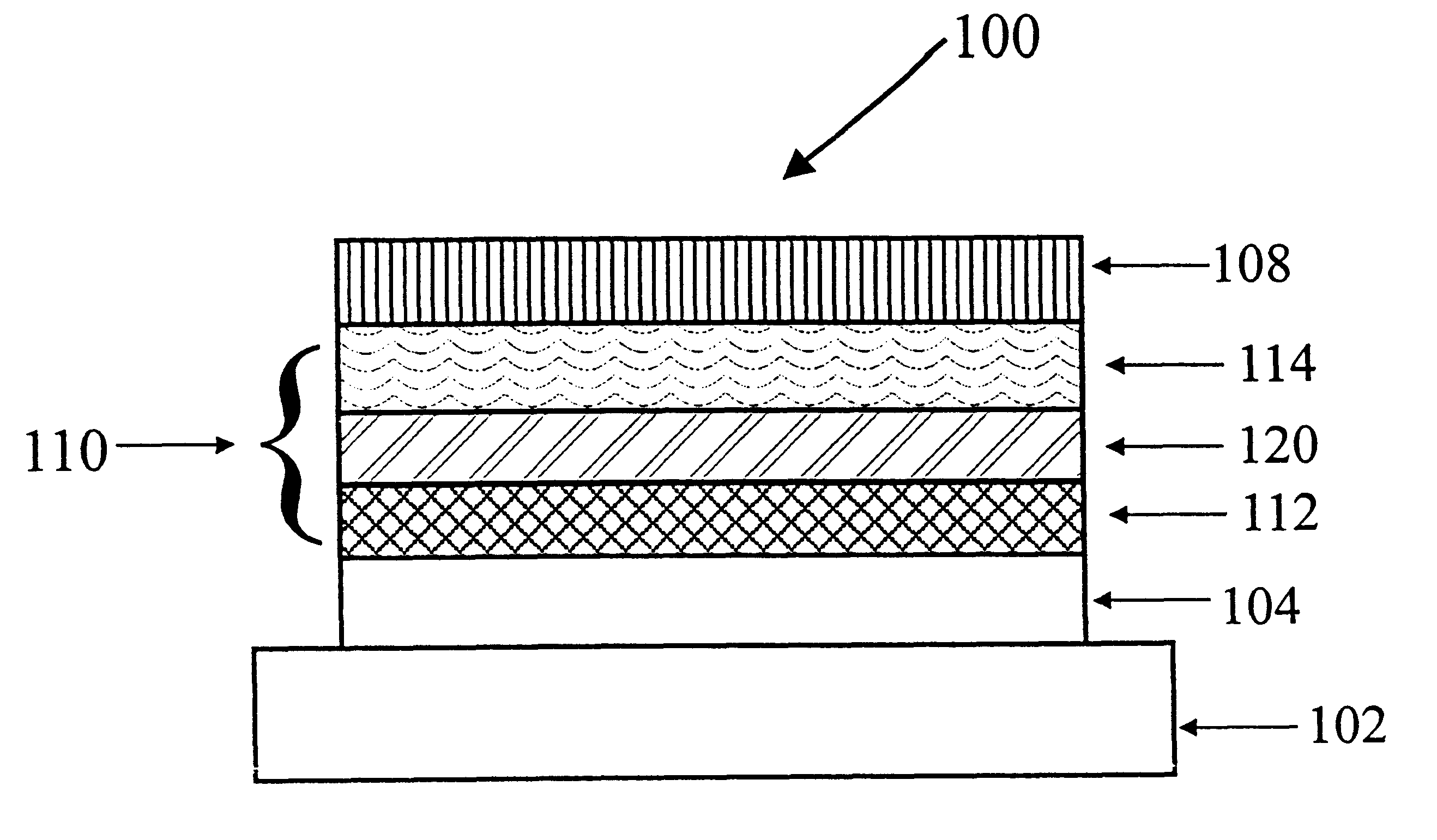
a) an ITO-coated glass was ultrasonically cleaned sequentially in a commercial detergent, iso-propanol, ethanol, and methanol, rinsed in deionized water, and then dried in an oven. The substrate was further subjected to a UV-ozone treatment for 10-20 minutes;
b) the substrate was put into a vacuum chamber, and the chamber was pumped down to 6.times.10.sup.-6 mbar;
c) a 70 nm thick NPB hole-transporting layer was deposited on ITO;
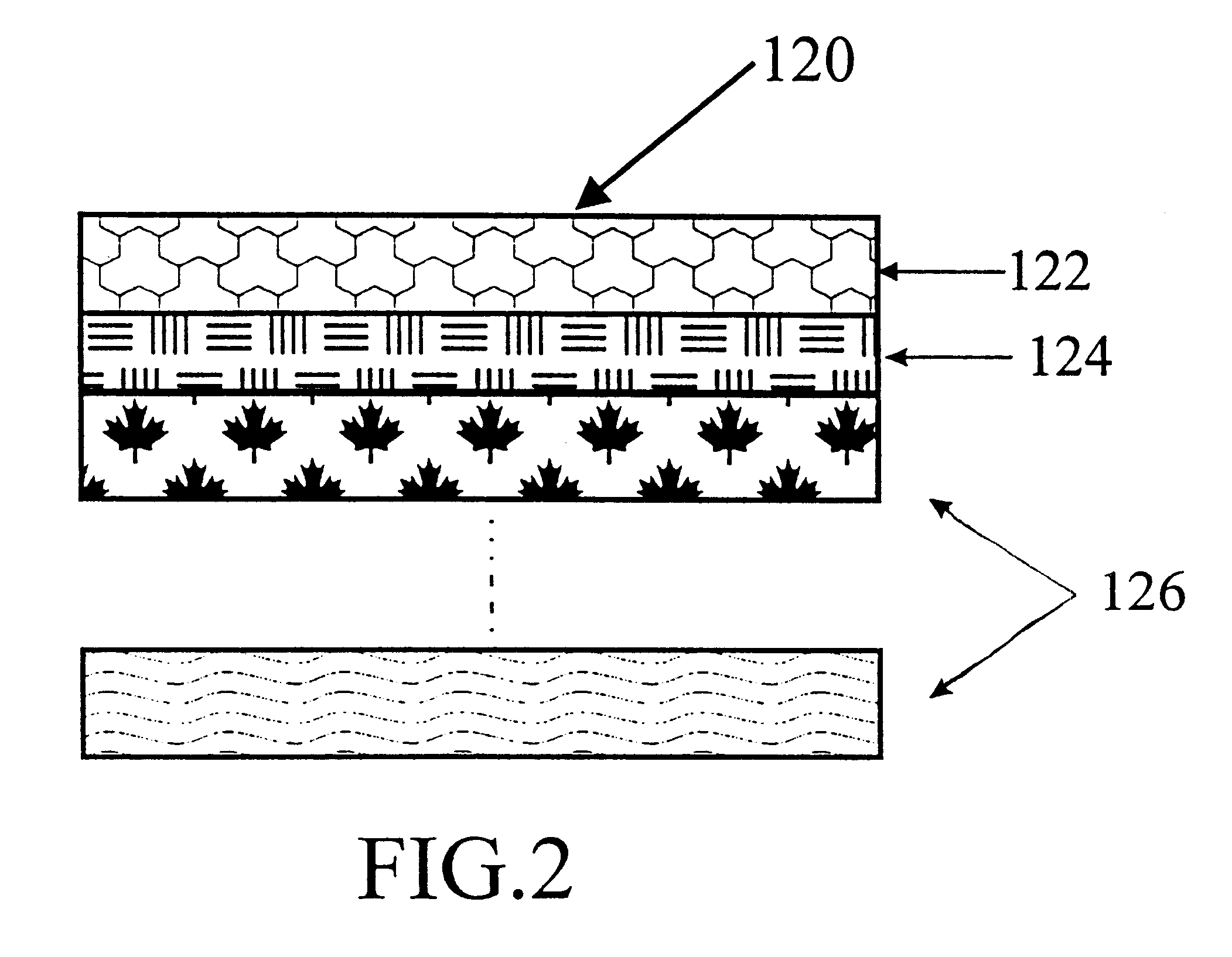
d) a 3.5 nm thick PDBT emitting sub-layer was deposited on TPD layer;
e) a 30 nm thick DPBI:PDBT(2%) emitting sub-layer was deposited on PDBT layer;
f) a 30 nm thick DPBI electron-transporting layer was deposited on DPBI:PDBT(2%) layer;
g) a 200 nm thick MgAg layer was deposited on DPBI layer by co-evaporation from two sources (Mg and Ag).
The electrical and optical properties of the device were characterized. The threshold voltage (define as the voltage at which the device emits light with a luminance of 1 cd / m.sup.2) was determined to be 5.5 V. The luminance was...
example 2
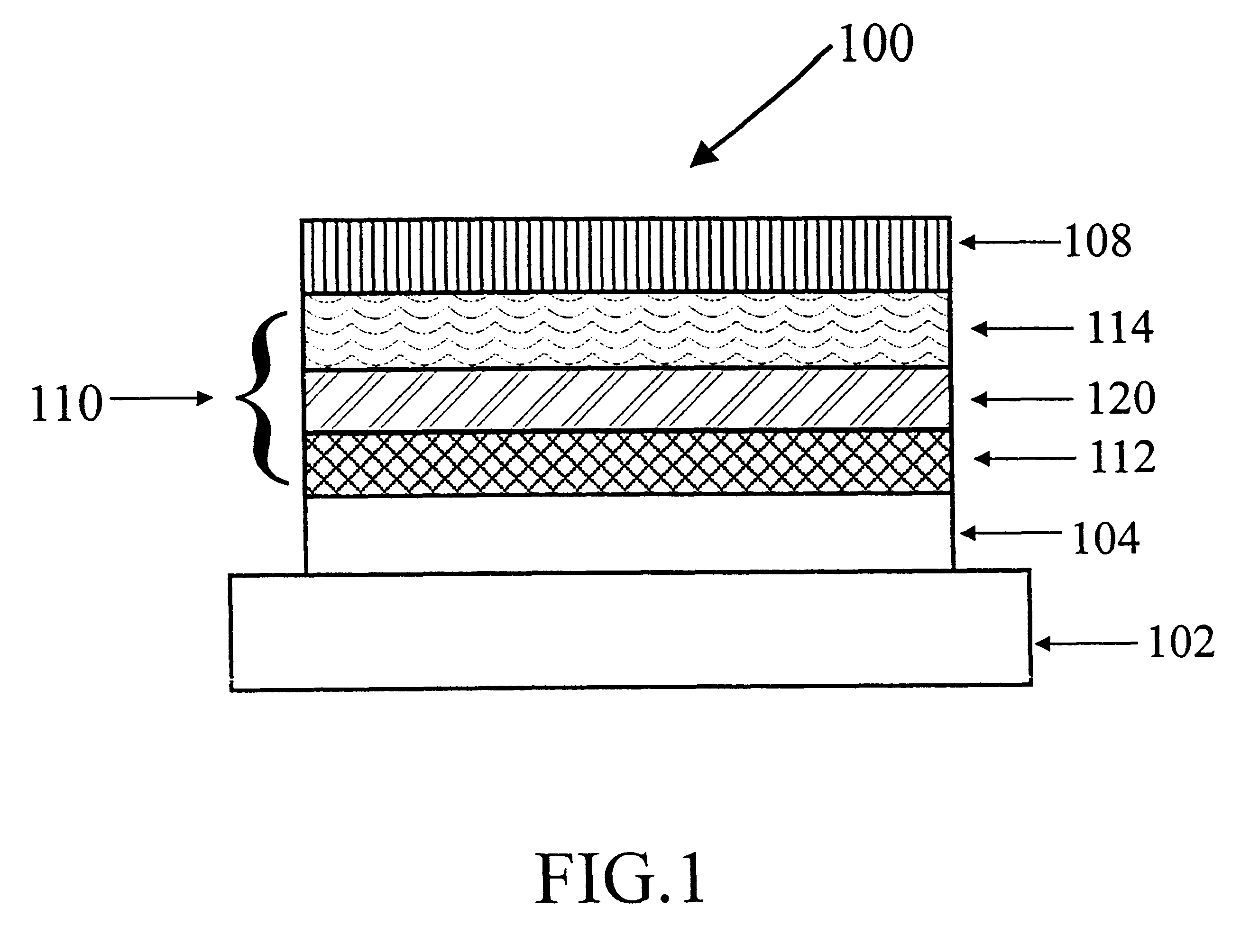
a) an ITO-coated glass was ultrasonically cleaned sequentially in a commercial detergent, iso-propanol, ethanol, and methanol, rinsed in deionized water, and then dried in an oven. The substrate was further subjected to a UV-ozone treatment for 10-20 minutes;
b) the substrate was put into a vacuum chamber, and the chamber was pumped down to 5.times.10.sup.-6 mbar,
c) a 70 nm thick NPB hole-transporting layer was deposited on ITO;
d) a 1.5 nm thick PDBT emitting sub-layer was deposited on TPD layer;
e) a 30 nm thick DPBI:PDBT(2%) emitting sub-layer was deposited on PDBT layer;
f) a 30 nm thick DPBI electron-transporting layer was deposited on DPBI:PDBT(2%) layer;
g) a 200 nm thick MgAg layer was deposited on DPBI layer by co-evaporation from two sources (Mg and Ag).
The electrical and optical properties of the device were characterized. The threshold voltage was determined to be 5.2 V. The luminance was 240 cd / m.sup.2 at 20V, 165 mA / cm.sup.2. The CIE 1930 is x=0.271,y=0.350. FIG. 5 shows th...
example 3
a) an ITO-coated glass was ultrasonically cleaned sequentially in a commercial detergent, iso-propanol, ethanol, and methanol, rinsed in deionized water, and then dried in an oven. The substrate was further subjected to a UV-ozone treatment for 10-20 minutes;
b) the substrate was put into a vacuum chamber, and the chamber was pumped down to 5.times.10.sup.-6 mbar;
c) a 70 nm thick NPB hole-transporting layer was deposited on ITO;
d) a 30 nm thick DPBI:PDBT(2%) emitting sub-layer was deposited on TPD layer;
e) a 30 nm thick DPBI electron-transporting layer was deposited on DPBI:PDBT(2%) layer;
f) a 200 nm thick MgAg layer was deposited on DPBI layer by co-evaporation from two sources (Mg and Ag).
The electrical and optical properties of the device were characterized. The threshold voltage was determined to be 4.4 V. The luminance was 590 cd / m.sup.2 at 18V, 175 mA / cm.sup.2. The CIE 1930 is x=0.198,y=0.252. FIG. 6 shows the emission spectrum of the organic LED prepared in this Example.
PUM
| Property | Measurement | Unit |
|---|---|---|
| work function | aaaaa | aaaaa |
| thick | aaaaa | aaaaa |
| work function | aaaaa | aaaaa |
Abstract
Description
Claims
Application Information
 - R&D Engineer
- R&D Manager
- IP Professional
- Industry Leading Data Capabilities
- Powerful AI technology
- Patent DNA Extraction
Browse by: Latest US Patents, China's latest patents, Technical Efficacy Thesaurus, Application Domain, Technology Topic.
© 2024 PatSnap. All rights reserved.Legal|Privacy policy|Modern Slavery Act Transparency Statement|Sitemap