Organic light emitting diode and preparation method thereof, and display panel

A light-emitting diode and organic technology, applied in semiconductor/solid-state device manufacturing, electrical components, circuits, etc., can solve the problems of low light-emitting efficiency of organic light-emitting diodes, and achieve the effects of maintaining balance, improving capabilities, and quickly and effectively injecting

Pending Publication Date: 2021-10-01
WUHAN CHINA STAR OPTOELECTRONICS TECH CO LTD +1
View PDF8 Cites 0 Cited by
  • Summary
  • Abstract
  • Description
  • Claims
  • Application Information

AI Technical Summary

Problems solved by technology

[0004] The embodiment of the present application provides an organic light emitting diode and its preparation method, so as to improve the problem of low luminous efficiency of organic light emitting diodes prepared from p-type doped materials

Method used


Image

  • Organic light emitting diode and preparation method thereof, and display panel
  • Organic light emitting diode and preparation method thereof, and display panel
  • Organic light emitting diode and preparation method thereof, and display panel

Examples


Embodiment 1

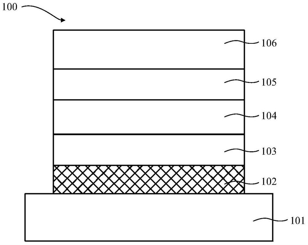
[0037] Such as figure 1 As shown, this embodiment provides an organic light emitting diode 100, the organic light emitting diode 100 is a top emission organic light emitting diode, the organic light emitting diode 100 includes: an anode layer 101, a hole injection layer 102, a hole transport layer 103 , the light emitting layer 104, the electron transport layer 105, and the cathode layer 106.

[0038] Wherein, the hole injection layer 102 is arranged on the surface of one side of the anode layer 101, and the hole injection layer 102 is used to inject holes from the cathode into the OLED device; the hole transport layer 103 is arranged on the hole The hole injection layer 102 is away from the surface of the anode layer 101 side, and the hole transport layer 103 is used to transport the holes injected into the OLED from the hole injection layer 102 to the light-emitting layer; the light-emitting layer 104 is arranged on the The surface of the hole transport layer 103 away from ...

Embodiment 2

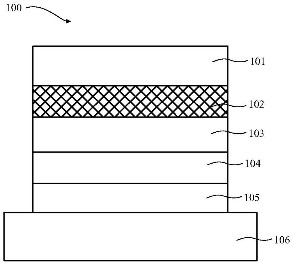
[0049] Such as figure 2 As shown, this embodiment provides an organic light emitting diode 100. The difference between the second embodiment of the present application and the first embodiment of the present application is that the organic light emitting diode 100 is a bottom-emitting organic light emitting diode; wherein, the The OLED 100 includes a cathode layer 106 , an electron transport layer 105 , a light emitting layer 104 , a hole transport layer 103 , a hole injection layer 102 and an anode layer 101 stacked from bottom to top.

[0050] Aiming at the technical problem of low efficiency of organic light emitting diodes prepared with p-type doped materials in the prior art, the embodiment of the present application provides a bottom emission type organic light emitting diode, the organic light emitting diode adopts poly(3,4-ethylene Dioxythiophene): The polymer host material composed of an aqueous solution of polystyrene sulfonate (PEDOT:PSS) and the additive material ...


PUM

PropertyMeasurementUnit
thicknessaaaaaaaaaa
electron work functionaaaaaaaaaa
thicknessaaaaaaaaaa

Abstract

Embodiments of the invention provide an organic light emitting diode and a preparation method thereof, and a display panel. The organic light emitting diode comprises an anode layer, a hole transport layer and a hole injection layer located between the anode layer and the hole transport layer, and the work function value of the hole injection layer is gradually increased in a direction from the anode layer to the hole transport layer; and therefore, an injection barrier between the anode layer and the hole transport layer is reduced, holes can be injected more quickly and effectively, hole injection capability is improved, and the luminous efficiency of the organic light emitting diode is further improved.

Description

technical field [0001] The present application relates to the field of display technology, in particular to an organic light emitting diode, a preparation method thereof, and a display panel. Background technique [0002] Organic Light Emitting Diode (OLED) is a photoelectric technology that uses organic semiconductor materials to produce reversible discoloration under current drive to achieve colorful display. OLED has the advantages of thinness, high brightness, active light emission, low energy consumption, large viewing angle, fast response, flexibility, and wide operating temperature range. It is considered to be the most promising new generation display technology. [0003] At present, the hole injection layer material in the OLED device structure is mainly realized by co-evaporating a p-type doped (p-dopant) material and a hole transport layer material. However, the preparation of current p-type doping materials is relatively complicated and costly, and the range of ...

Claims


Application Information

Patent Timeline
Patent Type & Authority Applications(China)
IPC IPC(8): H01L51/50H01L51/54H01L51/56H01L27/32
CPCH10K71/12H10K59/12H10K85/111H10K85/1135H10K50/17H10K71/00Y02E10/549
Inventor 相烨鹏
Owner WUHAN CHINA STAR OPTOELECTRONICS TECH CO LTD
Why Eureka
Try Eureka