Self-aligned non-volatile random access memory cell and process to make the same

Inactive Publication Date: 2003-02-25
SILICON STORAGE TECHNOLOGY +1
View PDF44 Cites 110 Cited by
  • Summary
  • Abstract
  • Description
  • Claims
  • Application Information

AI Technical Summary

Problems solved by technology

One of the problems facing the manufacturability of semiconductor floating gate memory cell arrays has been the alignment of the various components such as source, drain, control gate, and floating gate.

Method used


Image

  • Self-aligned non-volatile random access memory cell and process to make the same
  • Self-aligned non-volatile random access memory cell and process to make the same
  • Self-aligned non-volatile random access memory cell and process to make the same

Examples


Embodiment Construction

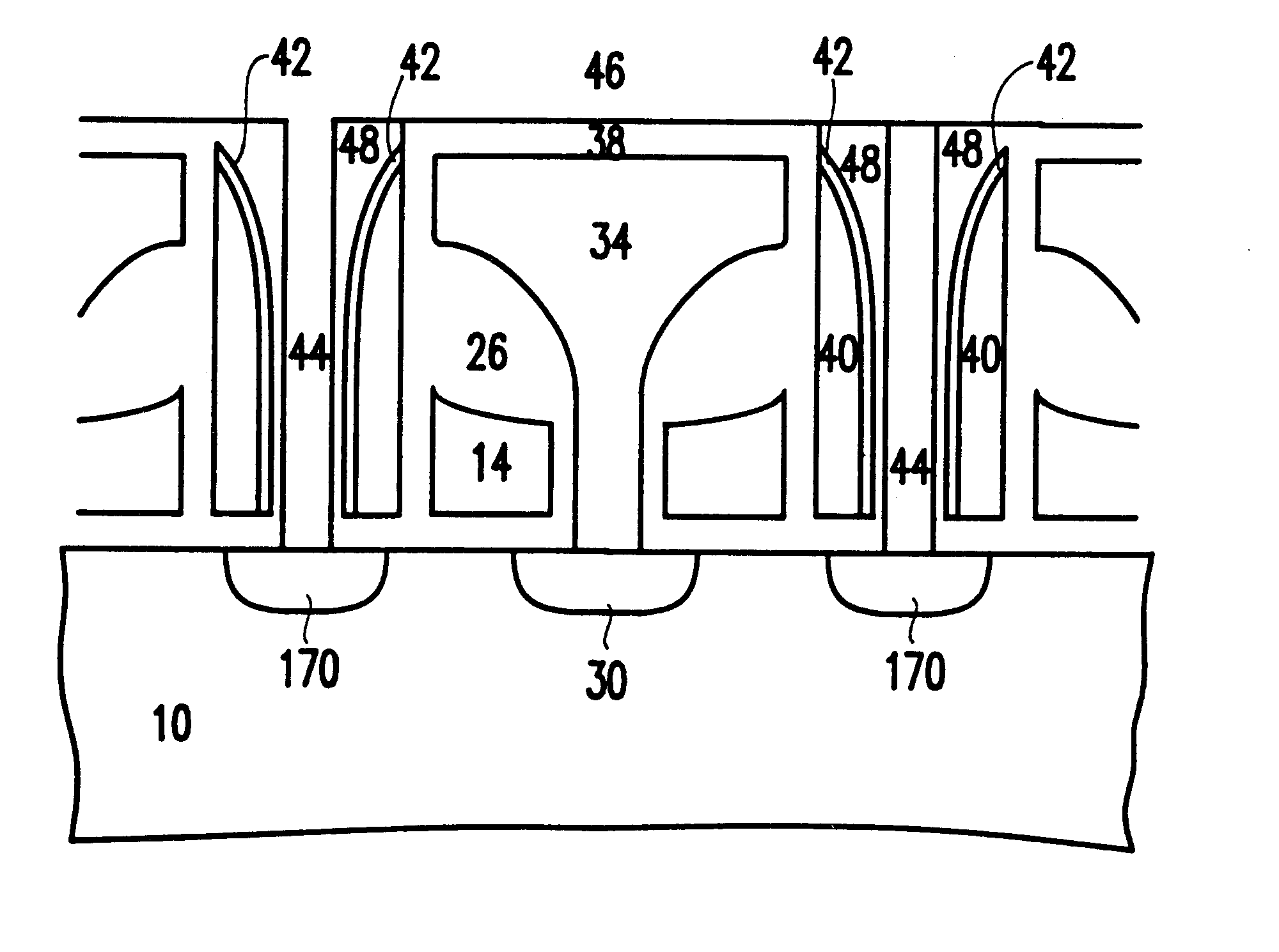
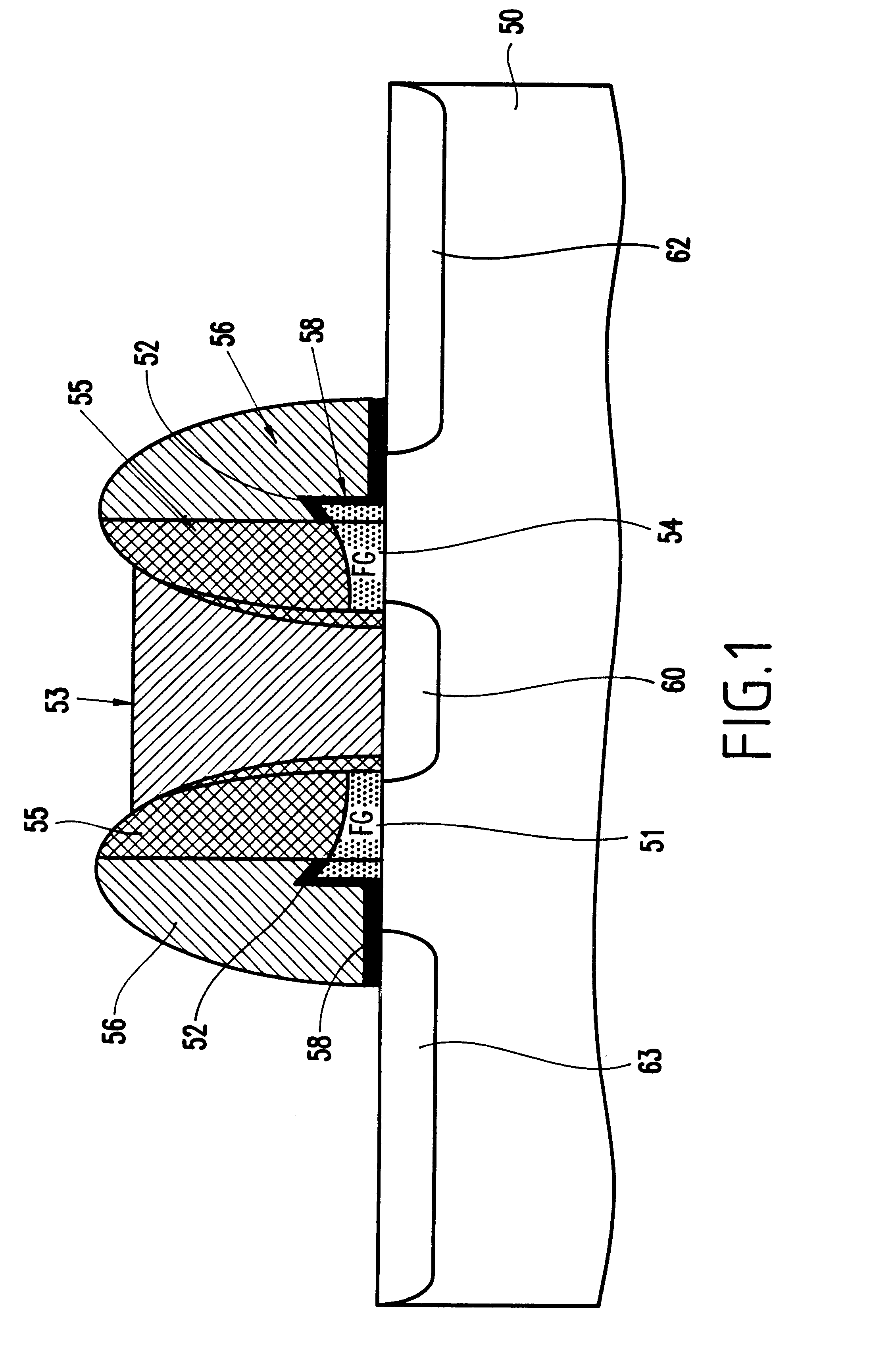
FIG. 1 shows the cell structure of a triple self-aligned NVRAM cell according to one embodiment of the present invention. Attributes of this structure include the polysilicon spacer wordline 56 which serves as the source side injection device, the sharp point 52 created by the floating gate (54 which is overlapped by tie dielectric material 58), and the self-aligned polysilicon source line contact 53 to the wordline.

As can clearly be seen in FIG. 1, the NVRAM cell according to one embodiment of the present invention has a unique structure. A silicon substrate 50 is provided having a doped source region 60, a doped bitline / drain region 62 and a doped bitline / drain region 63. A first polysilicon floating gate 51 and a second polysilicon floating gate 54 are provided over the substrate 50 and are both partly overlapping the source region 60. A polysilicon source line contact plug 53 is provided between the floating gates 51 and 54 to provide self-alignment with the floating gates.

The f...


PUM


Abstract

A self aligned method of forming a semiconductor memory array of floating gate memory cells in a semiconductor substrate has a plurality of spaced apart isolation regions on the substrate substantially parallel to one another. An active region is between each pair of adjacent isolation regions. The active and isolation regions are formed in parallel and in the column direction. In the row direction, strips of spaced apart silicon nitride are formed. A source line plug is formed between adjacent pairs of silicon nitride and is in contact with a first region in the active regions, and the isolation regions. The strips of silicon nitride are removed and isotropically etched. In addition, the materials beneath the silicon nitride are also isotropically etched. Polysilicon spacers are then formed in the row direction parallel to the source line plug and adjacent to the floating gates to form connected control gates. A second region is formed between adjacent, spaced apart, control gates. A bit line is formed in the bit line direction contacting the second region in the space between the control gates.

Description

1. Field of the InventionThe present invention generally relates to a self-aligned non-volatile memory and method of manufacture and more particularly relates to a triple-self-aligned split gate non-volatile random access memory (NVRAM) cell.2. Description of the Related ArtNon-volatile semiconductor memory cell using a floating gate to store charges thereon and memory arrays of such non-volatile memory cells formed in a semiconductor substrate are well known in the art. Typically, such floating gate memory cells have been of the split gate type, or stacked gate type, or a combination thereof.One of the problems facing the manufacturability of semiconductor floating gate memory cell arrays has been the alignment of the various components such as source, drain, control gate, and floating gate. As the scale of integration of semiconductor processing increases, reducing the largest lithographic feature, the need for precise alignment becomes more critical. Alignment of various parts al...

Claims


Application Information

Patent Timeline
Patent Type & Authority Patents(United States)
IPC IPC(8): H01L21/70H01L27/115H01L29/40H01L29/423H01L21/8247H01L29/788H01L29/792
CPCH01L27/115H01L29/42324H01L27/11521H10B69/00H10B41/30
Inventor JOHNSON, JEFFREY B.LAM, CHUNG H.LEE, DANAMARTIN, DALE W.RANKIN, JED H.
Owner SILICON STORAGE TECHNOLOGY
Why Eureka
Try Eureka