
Extended drain MOSFET for programming an integrated fuse element to high resistance in low voltage process technology

a technology of integrated fuse elements and drain mosfets, which is applied in the field of fuse elements, can solve the problems of large silicon area, large silicon area, and small resistance change of fuse devices, and achieve the effect of consuming large silicon area

Inactive Publication Date: 2003-02-25
NAT SEMICON CORP
View PDF7 Cites 44 Cited by
  • Summary
  • Abstract
  • Description
  • Claims
  • Application Information

AI Technical Summary

Benefits of technology

In another embodiment, the trench is formed to have a depth and a surface width so that a parasitic resistance between the first diffusion region and the channel region is minimized.

Problems solved by technology

Further, the fuse device may exhibit only a small change in resistance between an unprogrammed state and a programmed state.
To that end, Bohr et al. uses relatively complex reference resistance and current mirror scheme which consumes large silicon area.

Method used


Image

  • Extended drain MOSFET for programming an integrated fuse element to high resistance in low voltage process technology
  • Extended drain MOSFET for programming an integrated fuse element to high resistance in low voltage process technology
  • Extended drain MOSFET for programming an integrated fuse element to high resistance in low voltage process technology

Examples


Embodiment Construction

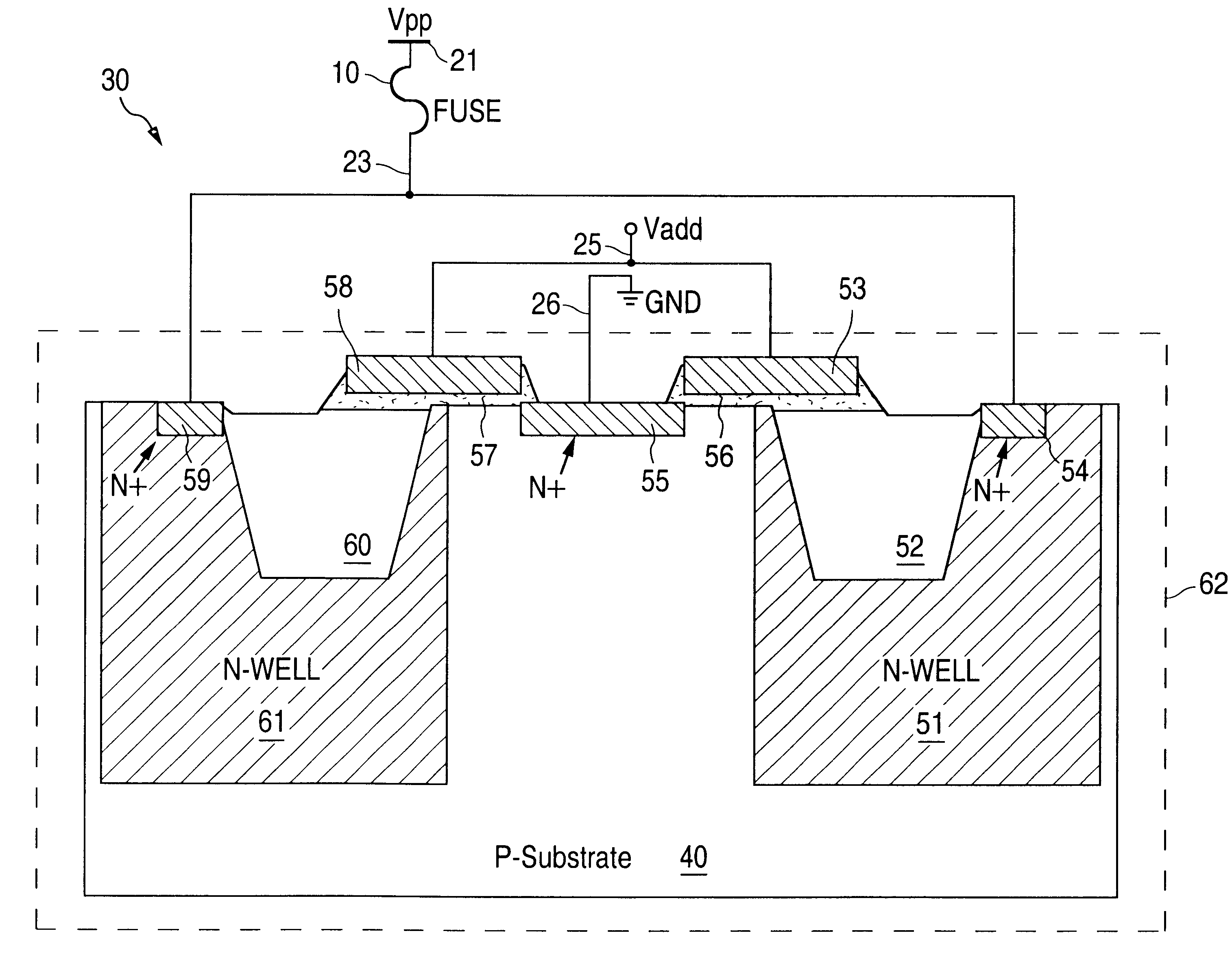
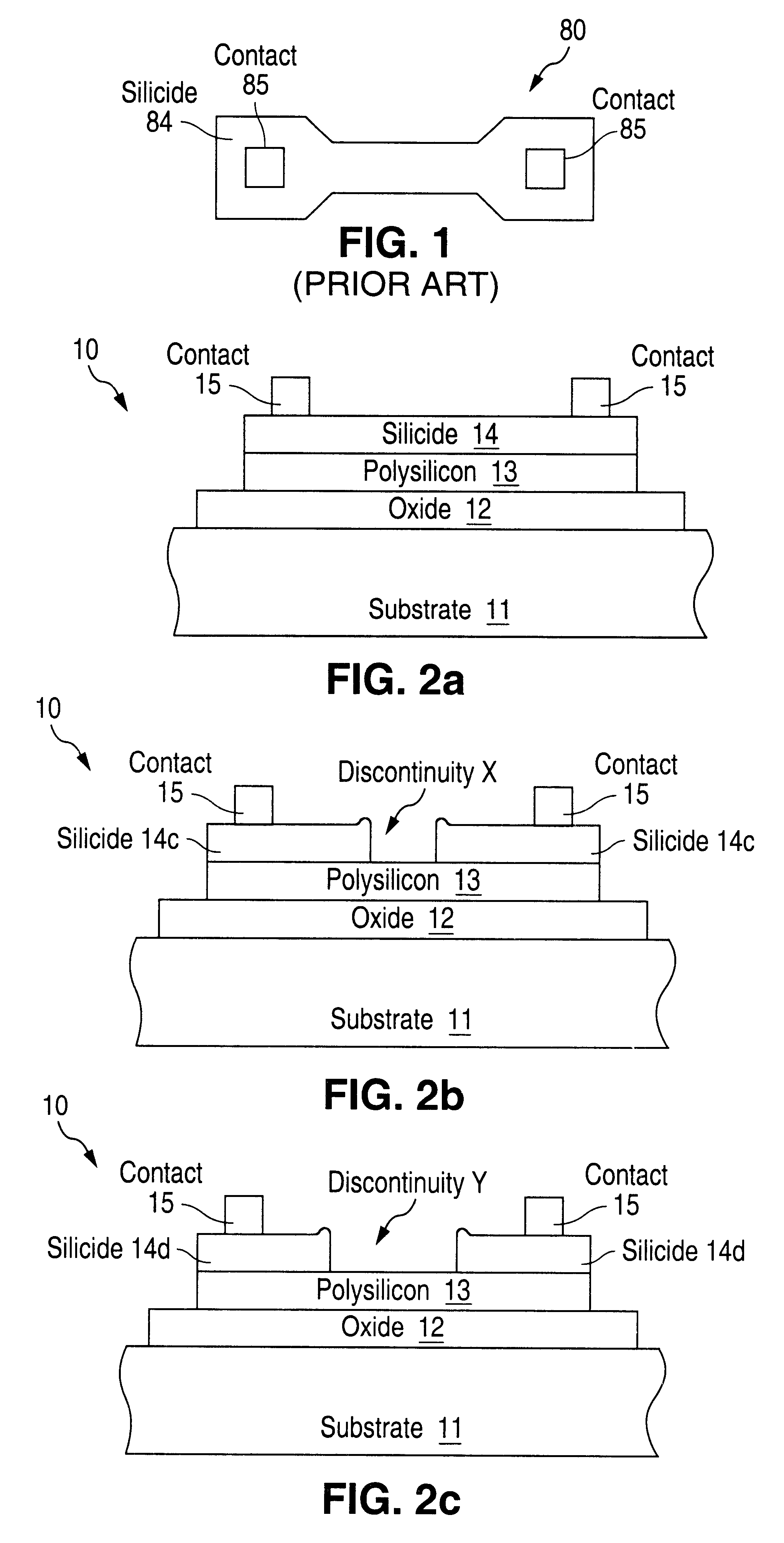
FIG. 2a shows a cross section of a fuse element 10 in accordance with the invention. Fuse 10 is a multi-layered structure which includes an insulating layer 12 over a substrate region 11, a polysilicon layer 13 over insulating layer 12, and a silicide layer 14 over and in contact with polysilicon layer 13. Contacts 15 are provided over silicide 14 to enable passing current through the silicide 14 and polysilicon 13 layers for programming fuse 10. Polysilicon 13 is undoped to maintain high resistance.

In its unprogrammed state (FIG. 2a), the resistance of fuse 10 is substantially equal to that of silicide 14, because the resistance of silicide is substantially less than that of polysilicon (by about a factor of 1.times.10.sup.5 to 1.times.10.sup.7 for undoped polysilicon).

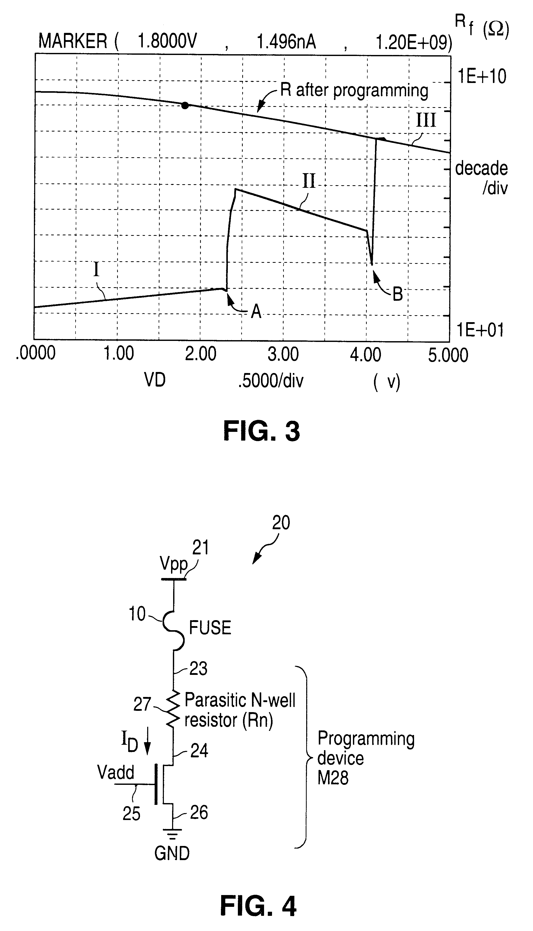
FIG. 3 shows the programming characteristics of fuse 10. The log of the fuse resistance R.sub.f (right vertical axis) is plotted against voltage V.sub.D (horizontal axis) applied across fuse 10. As V.sub.D is increas...


PUM


Abstract

An integrated fuse element is capable of being programmed to high resistance in low voltage process technology. The fuse includes a stack of an undoped polysilicon layer and a silicide layer. A voltage applied across the stack is increases until a first agglomeration event occurs, whereby a discontinuity is formed in the silicide layer. The current is further increased to cause a second agglomeration event whereby the size of the discontinuity is increased. Each agglomeration event increases the resistance of the fuse. An extended-drain MOS transistor, capable of sustaining high voltage, is connected in series with the fuse for programming the fuse. The transistor includes: a well region in a substrate, the well region forming the drain of the transistor; an insulating trench in the well; and a polysilicon gate extending over a portion of the substrate, a portion of the well and a portion of the trench, wherein upon reverse-biasing the junction between the well and the substrate a depletion region is formed which encompasses at least the entire portion of the surface region of the well over which the polysilicon extends.

Description

1. Field of the InventionThe invention relates to fuse elements used in semiconductor devices, and more particularly to an integrated fuse element capable of being programmed to high resistance in low voltage process technology.2. Description of Related ArtFuses are frequently used in integrated circuits to permanently store information, or to form the desired interconnections after the integrated circuit is manufactured.A fuse 80 is shown in FIG. 1. Fuse 80 and the corresponding programming and sensing circuitries are described in detail in the patent issued to Bohr et al. (U.S. Pat. No. 5,708,291, issued Jan. 13, 1998). The fuse device of Bohr et al. has a low programming voltage, and thus, a low programming current. This requires that the sensing circuit used to sense whether the fuse has been programmed or burned, does not burn (i.e. program) an unburned (i.e. unprogrammed) fuse in the sensing process. Further, the fuse device may exhibit only a small change in resistance betwee...

Claims


Application Information

Patent Timeline
Patent Type & Authority Patents(United States)
IPC IPC(8): H01L23/52H01L23/525H01L27/10
CPCH01L23/5256H01L27/101H01L2924/0002H01L2924/00H10B20/25
Inventor KALNITSKY, ALEXANDERPOPLEVINE, PAVELBERGEMONT, ALBERT
Owner NAT SEMICON CORP
Features
  • Generate Ideas
  • Intellectual Property
  • Life Sciences
  • Materials
  • Tech Scout
  • Unparalleled Data Quality
  • Higher Quality Content
  • 60% Fewer Hallucinations
Learn More