Image forming apparatus

a technology of forming apparatus and forming tube, which is applied in the direction of discharge tube luminescnet screen, tube with electrostatic control, tube with screen, etc., can solve the problems of weight, cathode electron-emitting device rapid response, and substrate heat melting not easy to occur

Inactive Publication Date: 2003-04-01
CANON KK
View PDF40 Cites 24 Cited by
  • Summary
  • Abstract
  • Description
  • Claims
  • Application Information

AI Technical Summary

Problems solved by technology

In addition, even if a multitude of electron-emitting devices are arranged on a substrate in high density, heat-melting of the substrate does not easily occur.
Further, different from the thermionic cathode electron-emitting devices that have slow response because they operate after being heated, the cold cathode electron-emitting devices have quick response.
In this flat-type CRT, the weight has been a serious problem.
Since the airtight container must have strength against approximately 1 atm to maintain this inner pressure, it needs thick constituent parts (e.g., face plate, rear plate and side walls), thus the weight of the container is great.
Thus, the weight of the flat-type CRT can be reduced by providing the support members, however, still there are problems such as the following:
The quality of display image is degraded due to electrical charge on the support members.
The electrical charge on the support member changes the electric potential distribution, which disturbs the control of electron beams.
As a result, the degradation of image quality such as disabled luminance control of display images or deformation of image occur.
The spark discharge passes a great amount of current through the parts in an instant and damages the fluorescent material and electrodes.
In other words, the support members become resources of electric noise.
a. Irregularly-drifting noise intruded into a modulation circuit causes erroneous operation of the circuit. In the worst case, the noise damages the modulation circuit.
b. A modulation signal is leaked to other parts via the support members, causing degradation of image quality such as cross-talk in display images.
c. The load on the modulation circuit increases. In case of a conventional modulation circuit, driving power becomes insufficient due to this increased load, thus lowering the response speed.
Further, the modulation signal applied to each cathode is leaked to another cathode via the support member S. Furthermore, the conductivity given to the support members S increases resistance load upon the modulation circuit.
The operation of the electron-emitting device becomes unstable otherwise the life of the device becomes short.
That is, the electrical connection between the support members or parts in contact with the support members causes the following inconveniences
e. Application of irregularly-drifting noise makes the operation of the electron-emitting device unstable.
Further, in comparison with a case where noise does not intrude into the device, the life of the device becomes shorter.
This results in change of the luminance of display images.

Method used


Image

  • Image forming apparatus
  • Image forming apparatus
  • Image forming apparatus

Examples


first embodiment

[First Embodiment]

A first embodiment will be described in accordance with FIGS. 1-2, 9-11 and 13-19.

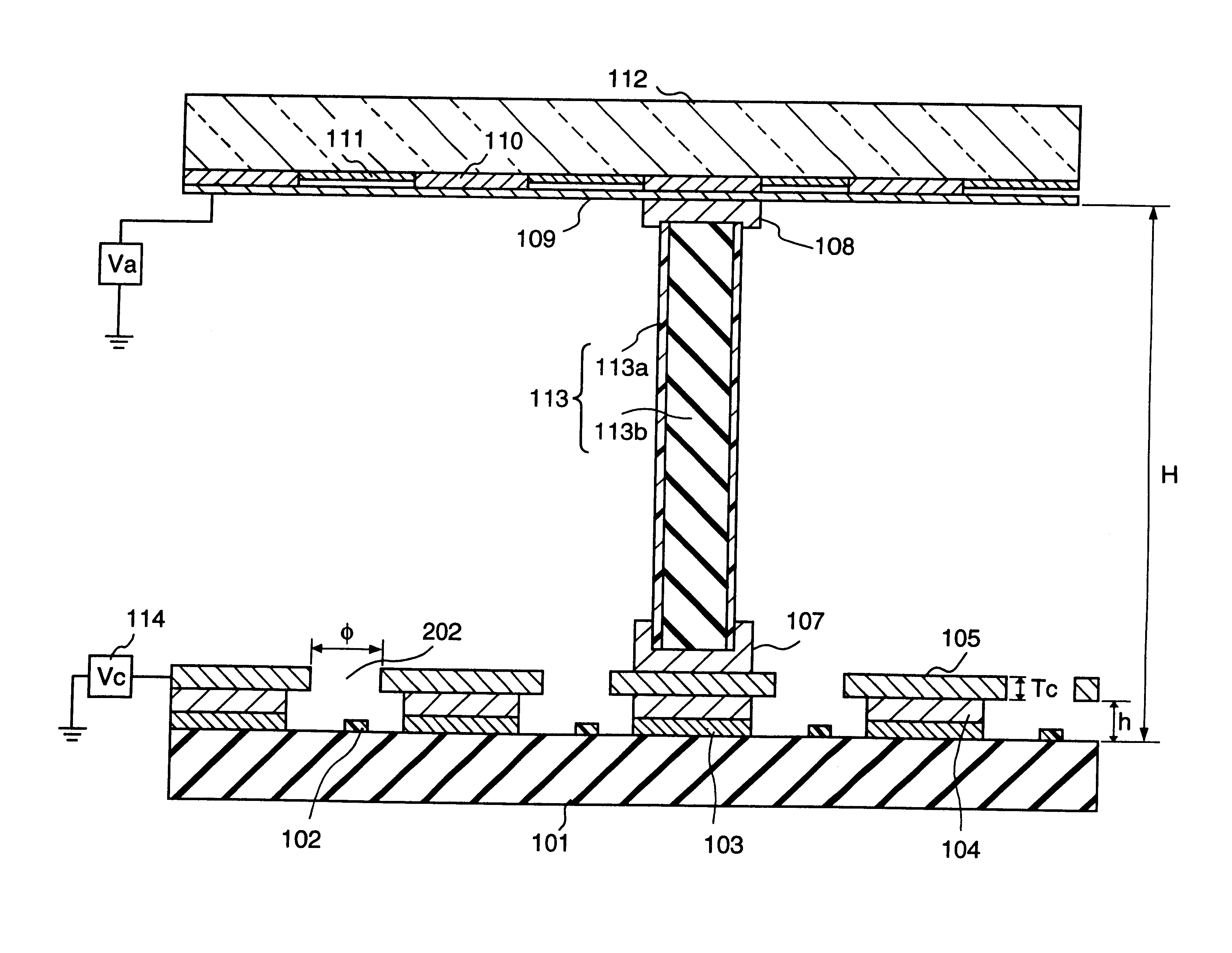
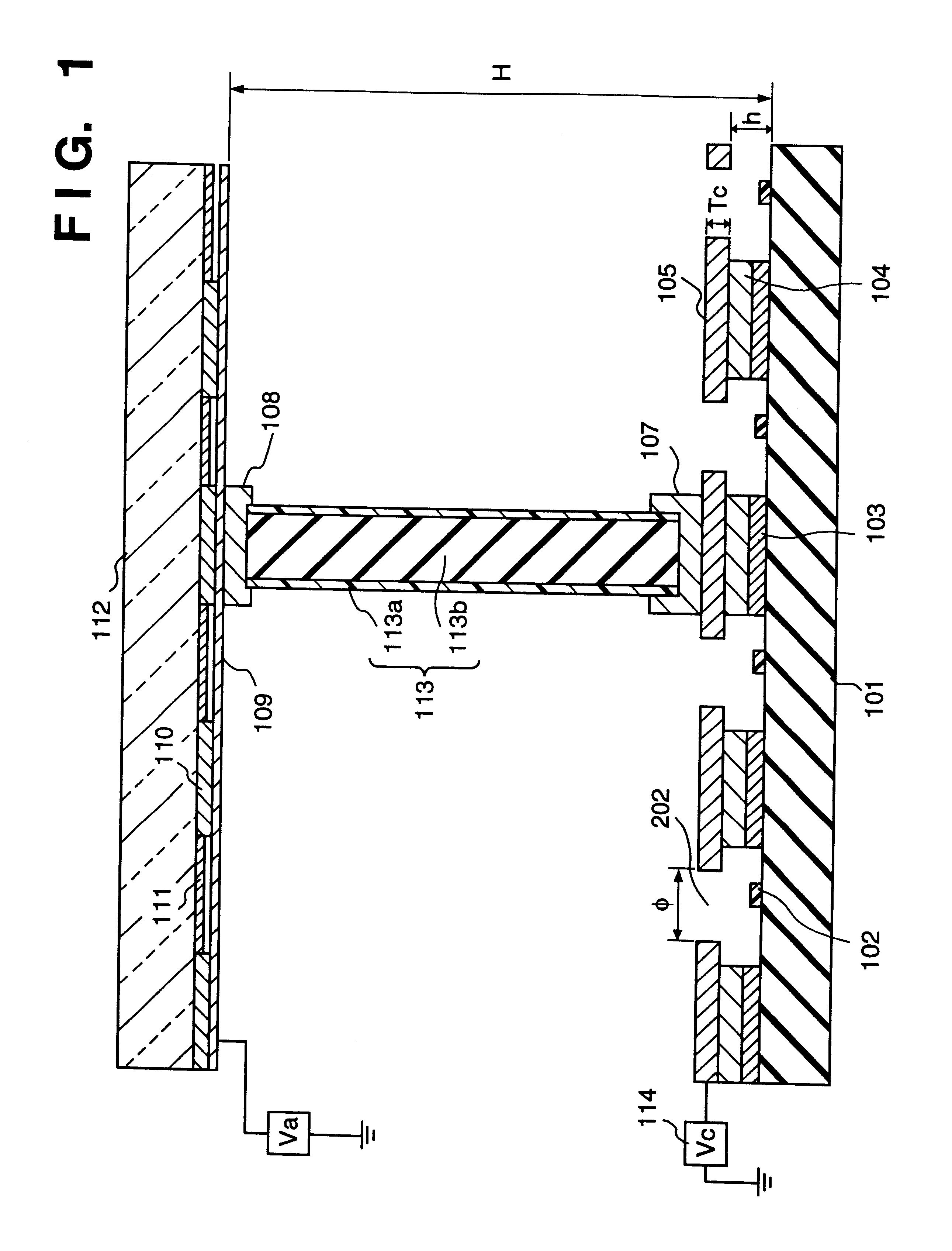
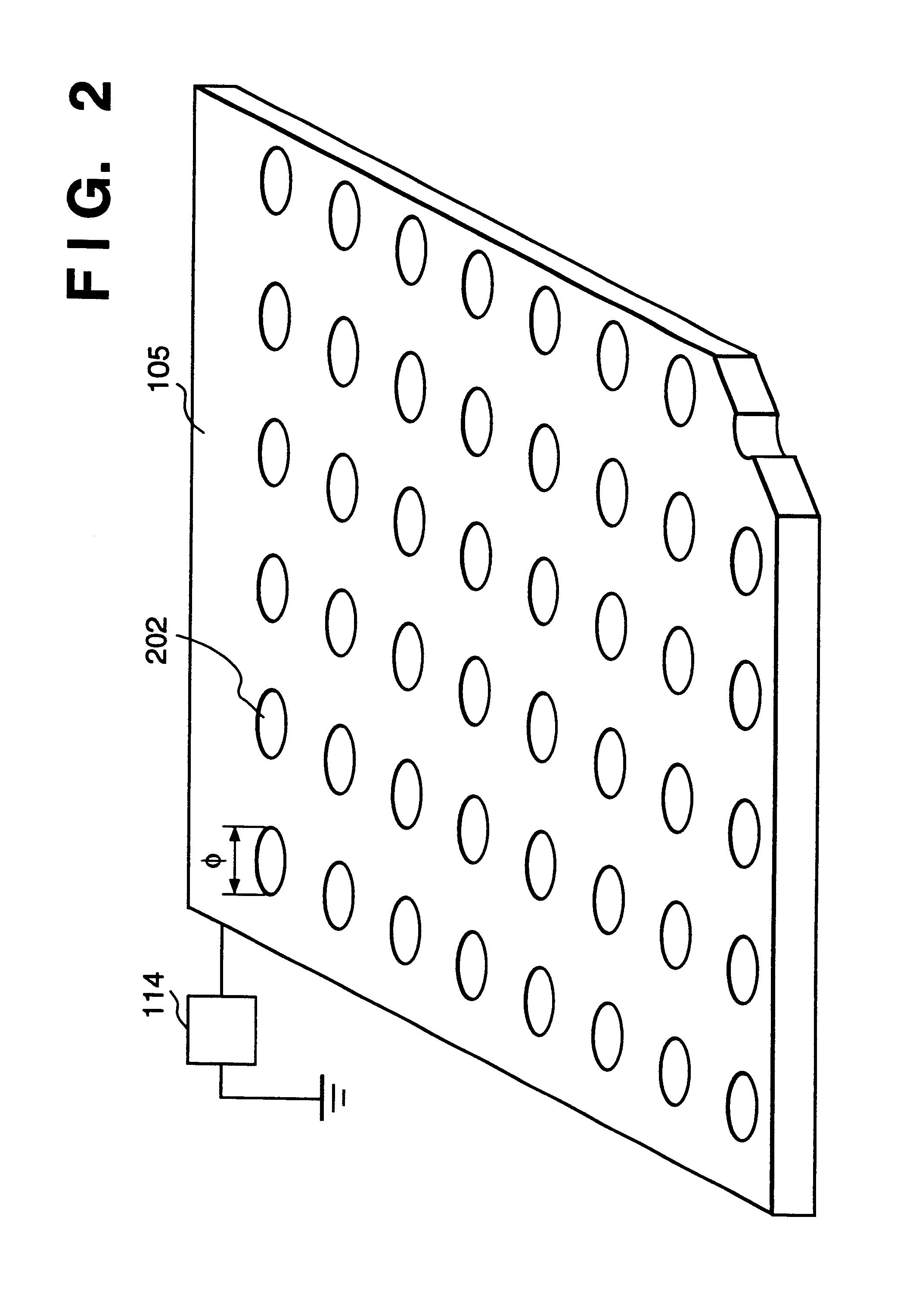
First, the basic structure of a display panel of a display apparatus will be described with reference to FIGS. 1 and 2. The structure and manufacturing method of the support members and potential-defining electrodes will be described in detail.

Then, a desirable shape of the second support members will be described with reference to FIGS. 13 and 14.

Next, the structure, manufacturing method and characteristic of the electron-emitting devices will be described with reference to FIGS. 9, 10 and 19.

Next, the construction and driving method of a multi electron-beam source having a matrix-wired electron-emitting devices will be described with reference to FIGS. 11, 16 to 18.

Finally, the construction of the display device circuit will be described with reference to FIG. 15.

First, the most characteristic feature of the present embodiment will be described using FIGS. 1 and 2. FIG. 1 shows the ...

second embodiment

[Second Embodiment]

FIG. 3 shows an image forming apparatus using the SCE type electron-emitting devices according to the second embodiment of the present invention. The present embodiment differs from the first embodiment, in that the potential-defining electrode 105 are formed only between the spacers 113 as the second support members, covered with the conductive films 113a, and the row-direction wiring electrodes 103. As the other parts of the structure are the same as those in the first embodiment, the explanation of those parts will be omitted. It has been confirmed the present embodiment has similar advantageous features to those in the first embodiment.

third embodiment

[Third Embodiment]

FIG. 4A shows a schematic perspective view of the image forming apparatus according to the third embodiment of the present invention. FIGS. 4B and 4C show cross-sectional views cut along a lines I--I and II--II in FIG. 4A respectively. In these figures, numeral 401 denotes a substrate; 404, column-direction wiring electrodes; 403, row-direction wiring electrodes formed on the column-direction wiring electrodes 404 via a insulating layer (not shown); 405, an insulating layer of frit glass; and 402, electron-emitting devices respectively having an electron-emitting portion 412. The electron-emitting devices 402 are electrically connected with the row-direction wiring electrodes 403 and the column-direction wiring electrodes 404, formed by screen printing silver (Ag) paste ink, via connection lines 406. Numeral 407 denotes a potential-defining electrode provided on the row-direction wiring electrodes 403 via the insulating layer 405. Different from the first embodimen...


PUM


Abstract

An image forming apparatus includes a first substrate and a second substrate disposed opposite to the first substrate, with fluorescent material being provided on the second substrate. A matrix wiring having a plurality of first wires and a plurality of second wires is provided, with each of the first wires located on the first substrate, and each of the second wires intersecting the plurality of first wires. Also included are electron-emitting devices, each of which emit an electron by applying a signal to the matrix wiring, and a metal electrode, having a plate-shaped form, provided above the matrix wiring, with the metal electrode having electron through-holes for passing electrons emitted by the electron-emitting devices. A support member, having a plate-shaped form, is provided on the metal electrode, wherein the metal electrode is arranged in parallel to the first substrate and a longitudinal direction of a cross section of the support member and a longitudinal direction of a cross-section of the metal electrode are perpendicular and intersect both of the metal electrode and the support member.

Description

1. Field of InventionThis invention relates to an image forming apparatus utilizing electron-emitting devices and, more particularly to an image forming apparatus in which a spacer as a support member is provided within the apparatus.2. Description of Related ArtConventionally, two types of electron-beam emitting devices, namely thermionic cathode electron-beam emitting devices and cold cathode electron-beam devices are known. Examples of cold cathode electron-emitting devices are electron-emitting devices of surface-conduction emission (hereinafter abbreviated to "SCE") type, field emission (hereinafter abbreviated to "FE") type, and metal / insulator / metal (hereinafter abbreviated to "MIM") type.A known example of the SCE type electron-emitting devices is described in "Radio Eng. Electron Phys., 10, 1290" (1965) by M. I. Elinson, and other examples will be described later.The SCE type electron-emitting device utilizes a phenomenon where electron-emission is produced in a small-area ...

Claims


Application Information

Patent Timeline
Patent Type & Authority Patents(United States)
IPC IPC(8): H01J31/12H01J29/02H01J29/87H01J29/06H01J29/62H01J29/82H01J29/86
CPCH01J29/028H01J29/864H01J31/127H01J2329/8655H01J2329/864H01J2329/8645H01J2201/3165
Inventor FUSHIMI, MASAHIROMITSUTAKE, HIDEAKISUZUKI, HIDETOSHI
Owner CANON KK
Why Eureka
Try Eureka