Method for forming a tantalum oxide capacitor

a technology of tantalum oxide and capacitor, which is applied in the direction of capacitors, semiconductor devices, electrical equipment, etc., can solve the problems of deterioration of electrical properties, step-coverage characteristics, and difficulty in miniaturizing semiconductor capacitors, and achieve the effect of improving the electrical characteristics of capacitors

Inactive Publication Date: 2003-04-22
SK HYNIX INC
View PDF8 Cites 29 Cited by
  • Summary
  • Abstract
  • Description
  • Claims
  • Application Information

AI Technical Summary

Benefits of technology

Methods for forming a tantalum oxide capacitor are disclosed, in which tantalum oxide is deposited by an atomic layer deposition ALD process so that the tantalum oxide layer is deposited uniformly on a lower electrode, whereby the step-coverage of the tantalum oxide layer is improved and accordingly the electrical characteristics of the capacitor are improved.
As described above, according to one disclosed method for forming a tantalum oxide capacitor, a tantalum-nitride layer is deposited by an atomic layer deposition ALD process and then a tantalum oxide layer is formed by oxidizing the tantalum-nitride layer, and therefore, the step-coverage of the tantalum oxide layer is improved and the electrical characteristics of the capacitor are improved.

Problems solved by technology

However, due to the limitation of the size required in storing a charge to satisfy a required capacitance, difficulties arise in miniaturizing semiconductor capacitors.
However, as the aspect ratio increases in the tantalum oxide layer according to the miniaturization of the device, the step-coverage characteristic deteriorates.
The reduction of the step-coverage may cause deterioration of the electrical properties of the capacitor, which cause reduction of capacitance of the capacitor.
Therefore, a capacitance sufficient to operate the semiconductor cannot be secured.
Furthermore, if the lower electrode is made of a metal, the tantalum oxide layer may not be deposited evenly due to the roughness of the surface of the metal, so there is a possibility that the tantalum oxide layer will become too thin in some locations.
Such a phenomenon causes a leakage current since the electric field is concentrated when a bias is applied.

Method used


Image

  • Method for forming a tantalum oxide capacitor
  • Method for forming a tantalum oxide capacitor
  • Method for forming a tantalum oxide capacitor

Examples


Embodiment Construction

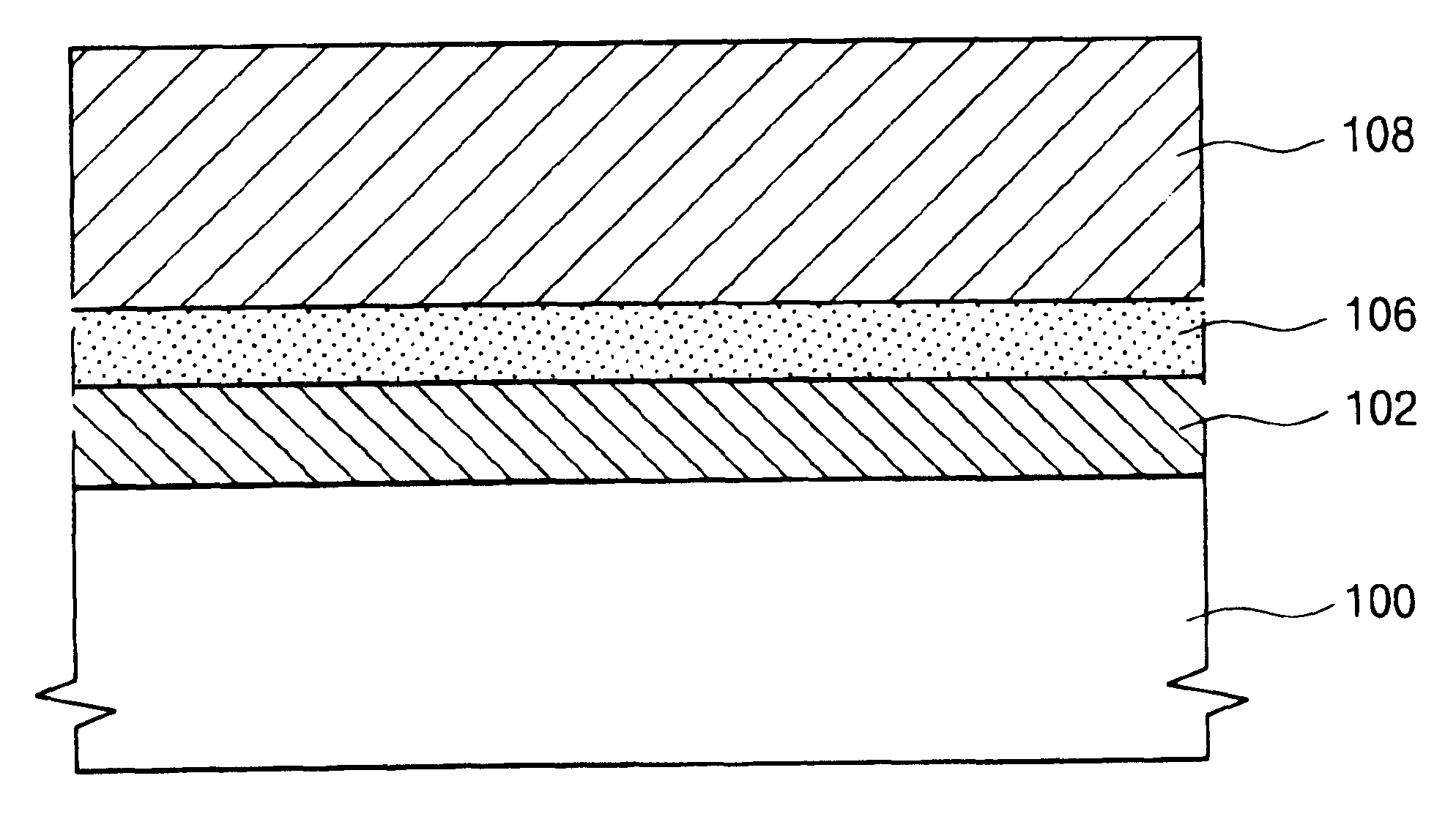
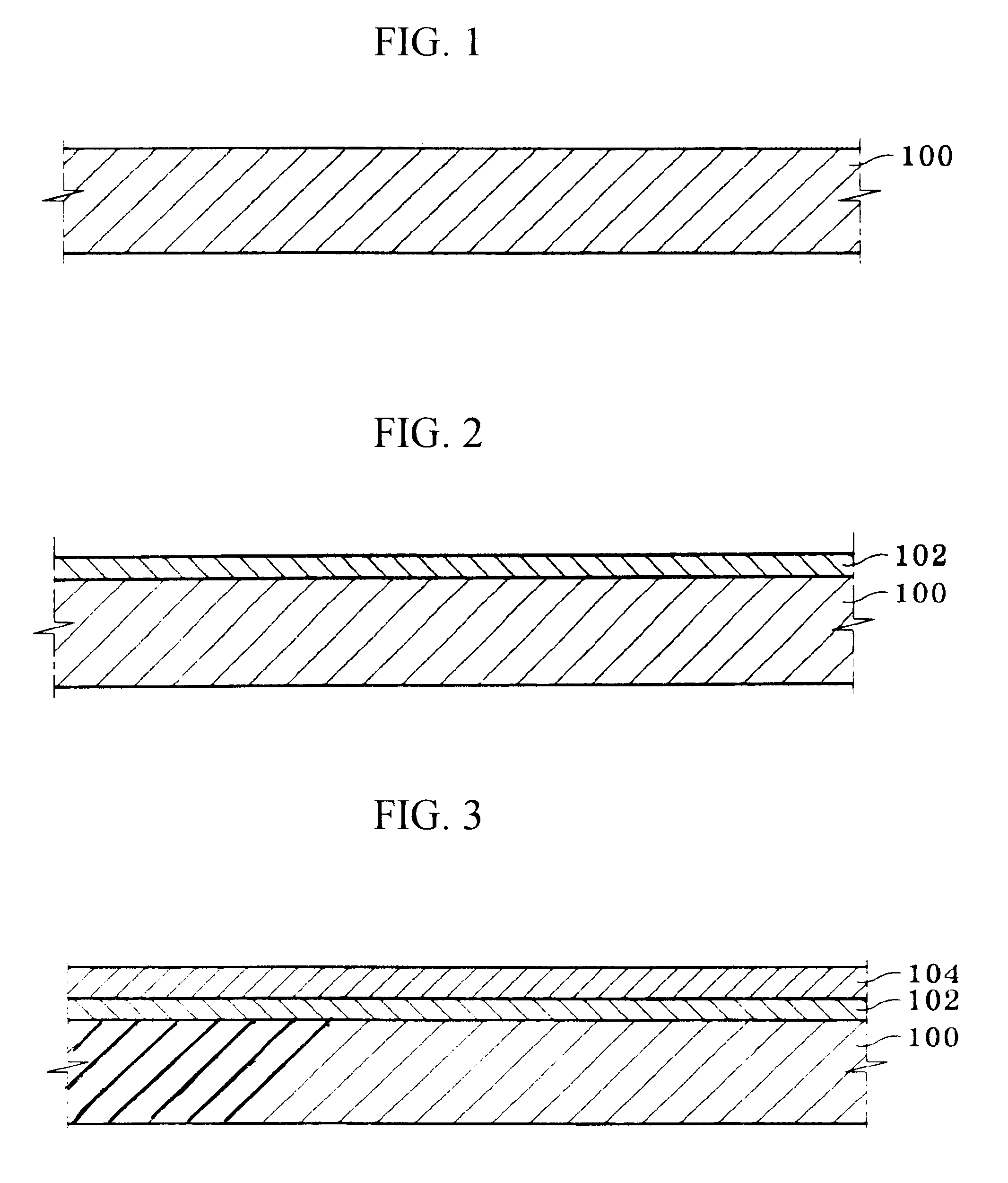
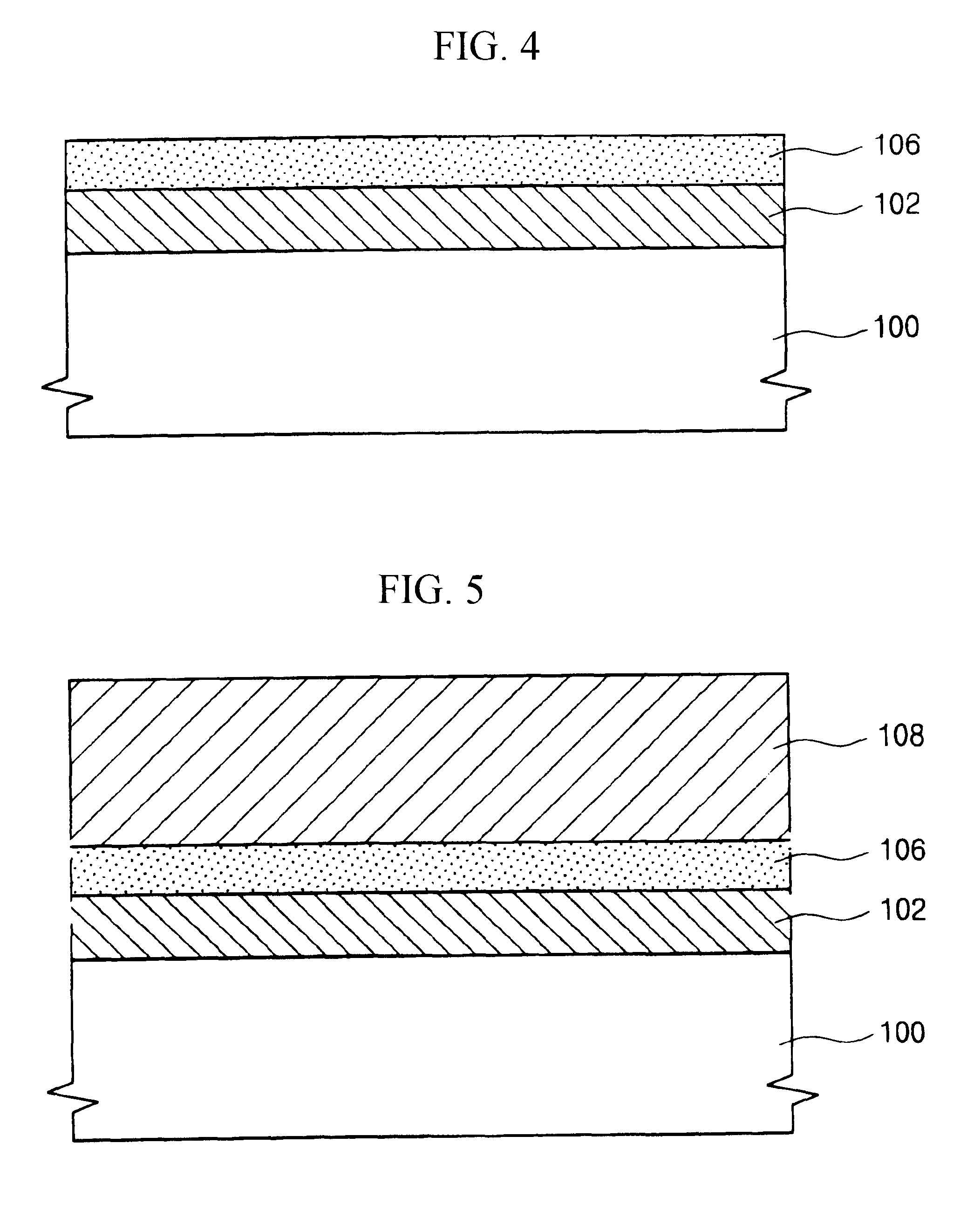
FIGS. 1 through 5 consecutively illustrate a disclosed process for manufacturing a tantalum oxide capacitor. In the drawings, the construction of the lower electrode 100 is shown as a single layer since that is not the main subject of this disclosure. Variations of the lower electrode 100 will be apparent to those skilled in the art.

According to one disclosed process, a nitride layer 102 is first formed on a lower electrode 100 by nitriding the upper part of the lower electrode 100.

More particularly, such a process prevents the forming of an oxide layer (silicon oxide) of low dielectric constant, which may be formed on an interface when a tantalum oxide layer 106 is deposited on the lower electrode 100, wherein the surface of polysilicon is nitrided by using a plasma under a NH.sub.3 atmosphere (or N.sub.2 / H.sub.2, N.sub.2 O atmosphere) at a temperature ranging from about 200 to about 600.degree. C., by an In-Situ process in a low pressure chemical vapor deposition chamber. In such...


PUM

PropertyMeasurementUnit
temperatureaaaaaaaaaa

Abstract

A method for forming capacitor using a tantalum oxide (TaO5) layer is disclosed. Tantalum oxide is deposited by an atomic layer deposition ALD process so that the step-coverage of the tantalum oxide layer is improved, and accordingly the electrical characteristics of the capacitor are improved.

Description

1. Technical FieldA method for forming a tantalum oxide capacitor is disclosed, and more particularly, a method for forming a tantalum oxide capacitor is disclosed in which tantalum oxide is deposited by an atomic layer deposition (ALD) process so that the step-coverage of the tantalum oxide layer is improved and accordingly the electrical characteristics of the resultant capacitor are improved.2. Description of the Related ArtIn general, a capacitor stores a charge and then supplies the charge required for the operation of a device, such as a semiconductor device. As the integration of the semiconductor devices increases, the size of the cells becomes smaller, and the capacitance required for the operation of the devices increases. The capacitance required in a semiconductor device having a greater integration than 64M DRAM is greater than 30 pF per cell.Also, as the integration of the semiconductor devices increases, miniaturization of capacitors has been required. However, due to...

Claims


Application Information

Patent Timeline
Patent Type & Authority Patents(United States)
IPC IPC(8): H01L21/02H01L29/66H01L21/316H01L27/08H01L29/94H01L27/04H01L21/822H01L21/8242H01L27/10H01L27/108
CPCH01L21/31604H01L21/31683H01L29/94H01L27/0805H01L28/40H01L21/02326H01L21/0228H01L21/02183H01L27/10H01L21/0234
Inventor PARK, DONG-SUKIM, HYUNG KYUN
Owner SK HYNIX INC
Why Eureka
Try Eureka