Semiconductor device and method therefor

a semiconductor and device technology, applied in the field of semiconductor device manufacturing, can solve the problems of mismatching crystalline structure of overlying semiconductor material, formation of misfit dislocation, and 4 percent mismatch in lattice constant of crystalline structur

Inactive Publication Date: 2003-06-10
NORTH STAR INNOVATIONS
View PDF7 Cites 110 Cited by
  • Summary
  • Abstract
  • Description
  • Claims
  • Application Information

AI Technical Summary

Problems solved by technology

The difficulty in this is that often the desired overlying semiconductor material has a mismatch in its crystalline structure with that of the underlying crystalline material.
The problem can occur for any situation in which there are two types of semiconductor materials desired for a particular integrated circuit, but currently a typical case is for the underlying semiconductor material to be silicon because that is the most common for making integrated circuits.
Germanium and silicon, however, have crystalline structures that have a 4 percent mismatch in the lattice constant.
The result of epitaxially growing a germanium layer over the silicon substrate is the formation of misfit dislocations.
The misfit dislocations in turn cause threading dislocations.
The threading dislocations create major problems with leakage and efficiency reduction of the photodetector.
A disadvantage of this technique is that a thick buffer layer is required to achieve the desired decrease in threading dislocations in the overlying germanium layer.
This results in a long and expensive deposition.
Additionally, the great difference in height of the silicon surface and the germanium surface will result in integration difficulties if an integrated circuit is to be fabricated from devices fabricated in the silicon surface and photodetectors in the germanium surface.
Because of the disadvantages of the graded buffer technique, there have been efforts to develop alternate techniques that reduce the threading dislocations in the overlying germanium layer but with substantial reduction in thickness of any intermediate layer.
This technique has been demonstrated to be beneficial in reducing threading dislocation densities, however the best reported results are not yet as good as those achieved with the graded buffer layer.
The use of multiple, high temperature thermal cycles, however, adversely affects any transistors that have already been formed in the integrated circuit.
Thus, the transistors formed in the silicon portion of the integrated circuit, prior to formation of the germanium layer, have substantially used up the available thermal budget.
The germanium layers grown with this technique, however, can result in no defects at many seams and in twins or low angle grain boundaries at other seams that have minimal impact on the electrical properties.
A disadvantage of this technique is that a thicker germanium layer must be deposited to first fill the holes and then to form the desired layer.
Additionally, if the holes and spaces are relatively large, the result is a rough surface that results in the growth of the germanium from the nucleation sites.
There are limitations, however, in the scaling that can be achieved with lithographic techniques.

Method used


Image

  • Semiconductor device and method therefor
  • Semiconductor device and method therefor
  • Semiconductor device and method therefor

Examples


Embodiment Construction

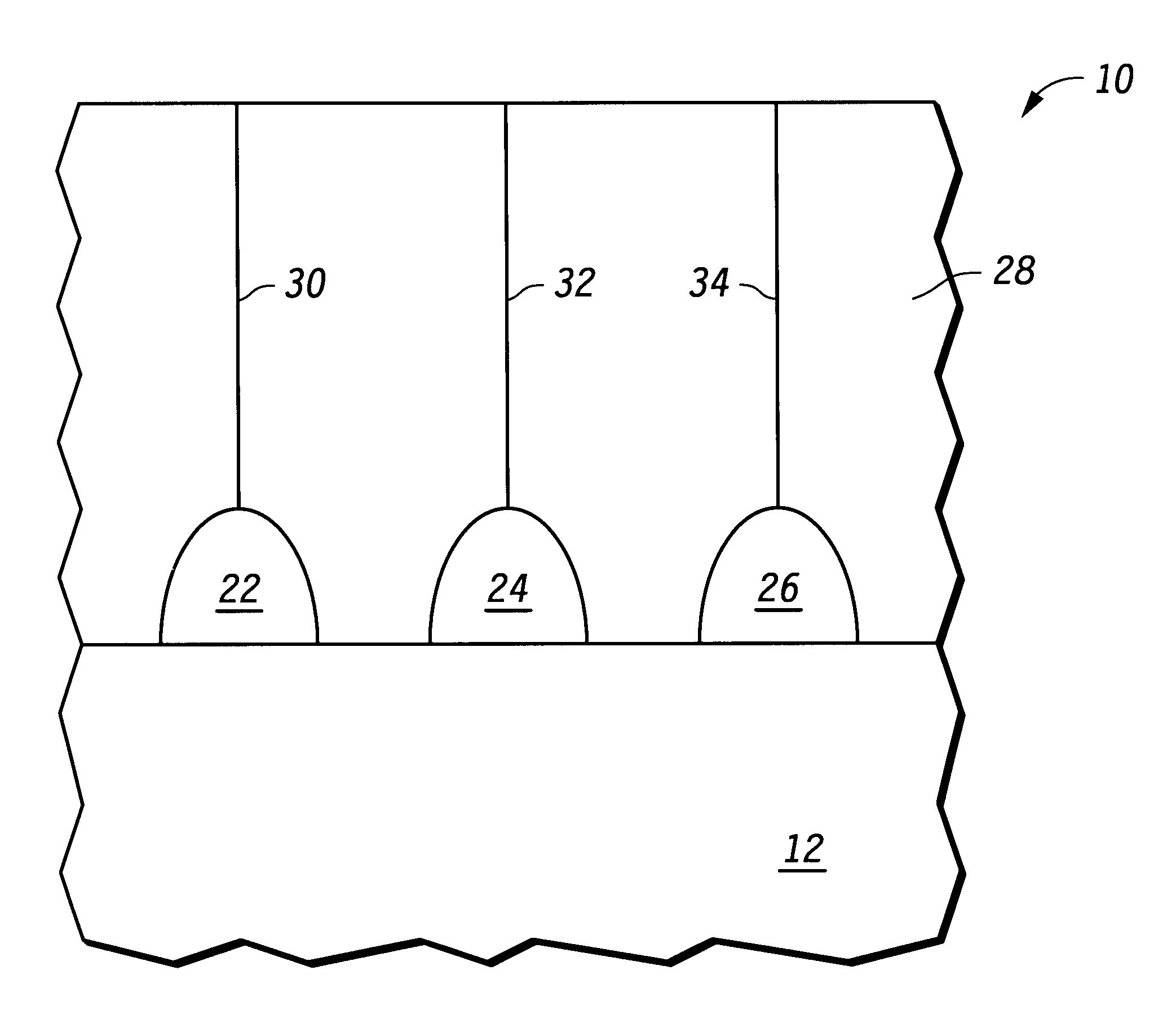
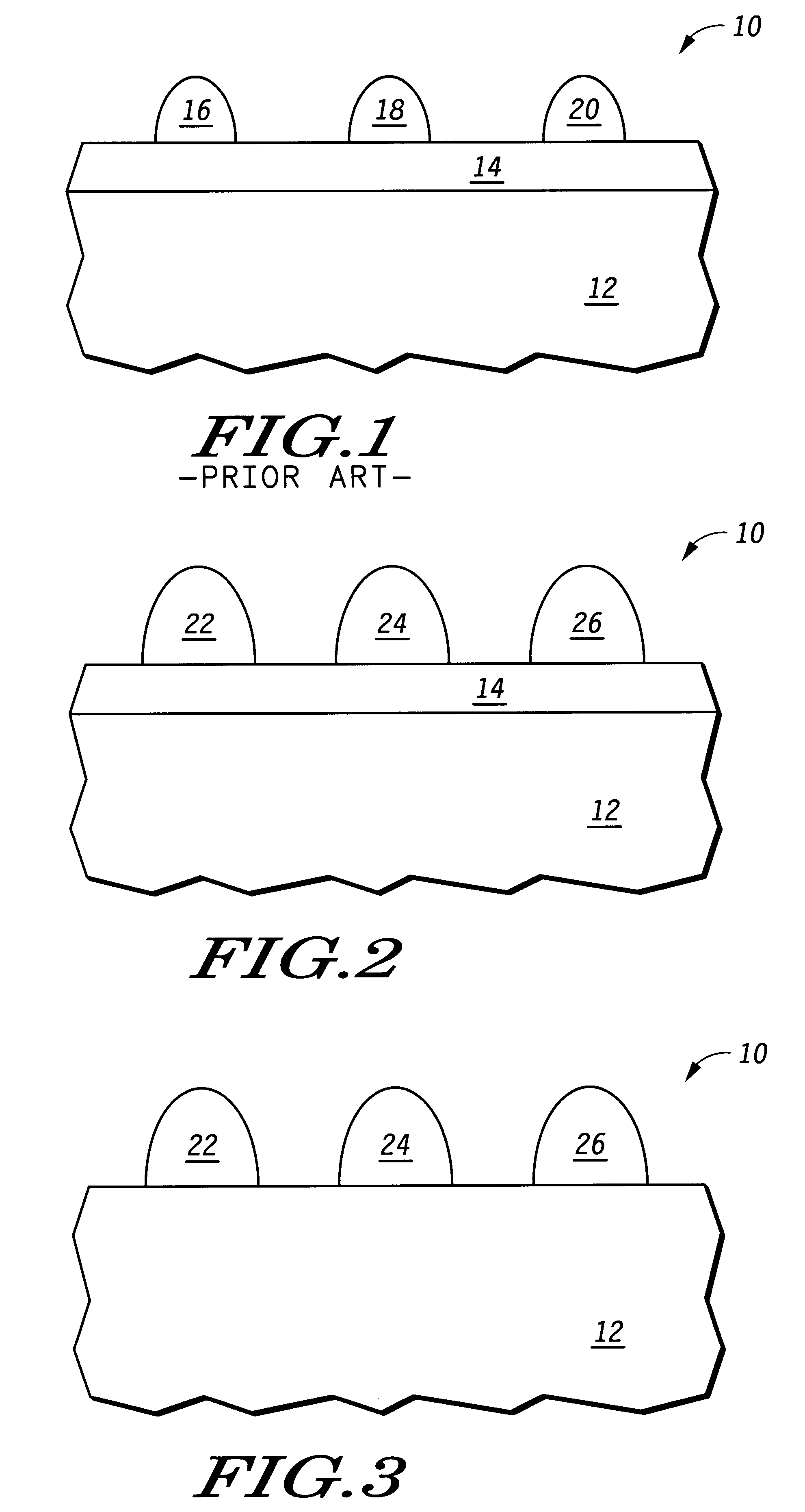
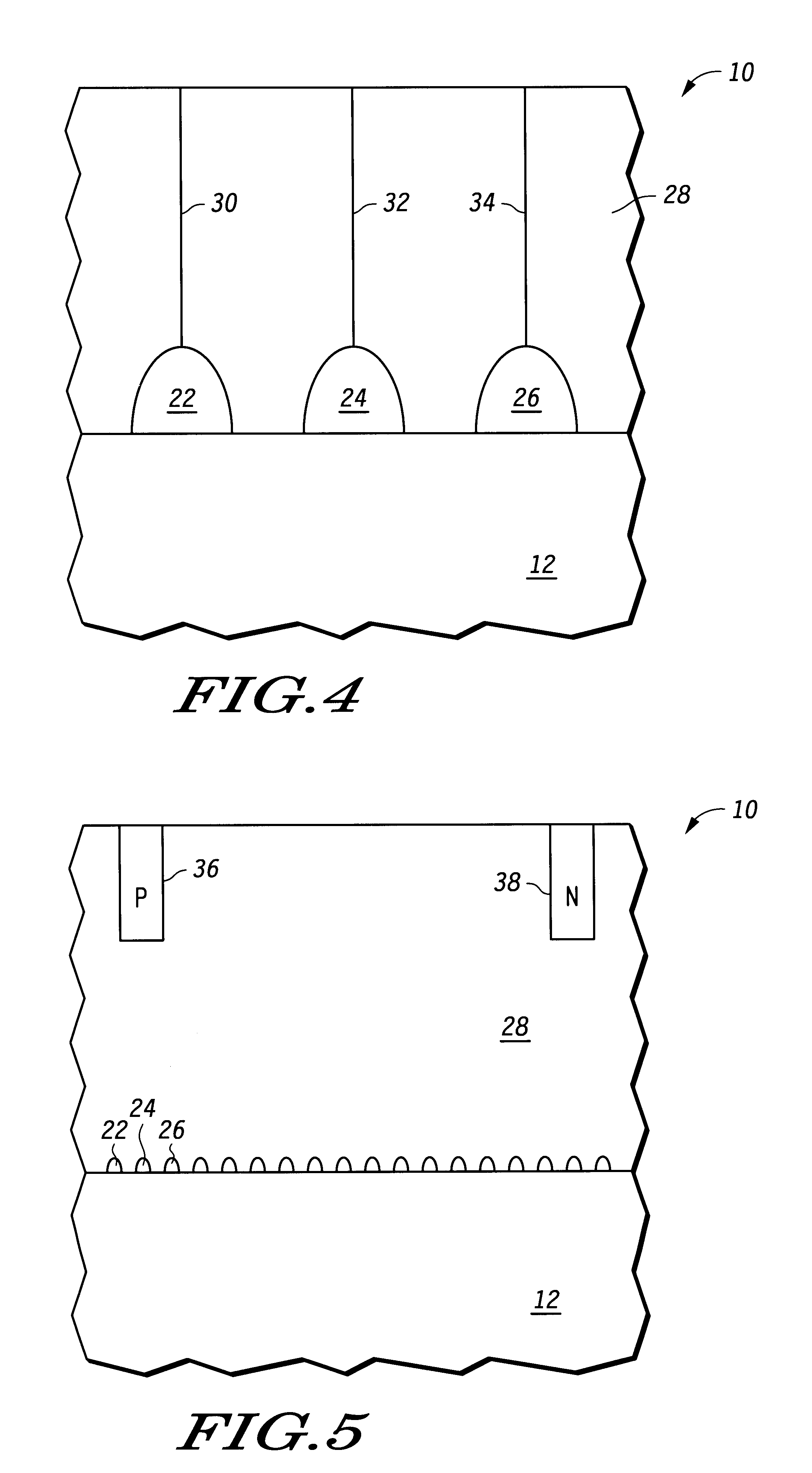
In one embodiment a photodetector using heteroepitaxial layers is formed in a portion of an integrated circuit using silicon nanocrystals that are formed relatively close together over a silicon substrate. These nanocrystals are completely oxidized to form insulating islands over the silicon. A subsequent etch back exposes the underlying silicon but leaves the insulating islands as masks for beginning a selective epitaxial growth of germanium over the silicon. The germanium grows and immediately forms misfit dislocations a short distance from the surface of the silicon. These misfit dislocations run a short distance above and parallel to the silicon substrate and are terminated at the insulating islands. The epitaxial growth continues and ultimately comes together at the top of these insulating islands. There may be a grain boundary formed at the top of each insulating island. The insulating islands are close enough together so that the misfit dislocations terminate on these islands...


PUM


Abstract

A heteroepitaxial structure is made using nanocrystals that are formed closer together than normal lithography patterning would allow. The nanocrystals are oxidized and thus selectively etchable with respect to the substrate and surrounding material. In one case the oxidized nanocrystals are removed to expose the substrate at those locations and selective epitaxial germanium is then grown at those exposed substrate locations. The inevitable formation of the misfit dislocations does minimal harm because they are terminated at the surrounding material. In another case the surrounding material is removed and the germanium is epitaxially grown at the exposed substrate where the surrounding material is removed. The resulting misfit dislocations in the germanium terminate at the oxidized nanocrystals. By using nanocrystals that are able to be formed much closer together than is available for other features through lithography, the misfits are prevented from extending so far as to create harmful threading dislocations.

Description

1. Field of the InventionThis invention relates to techniques for making semiconductor devices and more particularly to forming heteroepitaxial structures.2. Related ArtThere are a variety of uses in semiconductor manufacturing for heteroepitaxial structures, structures in which one type of semiconductor material is grown on the top of another type. The desire is for both the underlying semiconductor material and the overlying semiconductor material to be monocrystalline. The difficulty in this is that often the desired overlying semiconductor material has a mismatch in its crystalline structure with that of the underlying crystalline material. The problem can occur for any situation in which there are two types of semiconductor materials desired for a particular integrated circuit, but currently a typical case is for the underlying semiconductor material to be silicon because that is the most common for making integrated circuits. In the case of optical electronics, it is desirable...

Claims


Application Information

Patent Timeline
Patent Type & Authority Patents(United States)
IPC IPC(8): H01L21/02H01L21/20H01L29/02H01L31/0352H01L29/165H01L31/0248H01L31/18
CPCH01L21/02381H01L21/02532H01L21/02543H01L21/02546H01L21/02647H01L29/165H01L31/0352H01L31/1804H01L21/02639Y02E10/547Y02P70/50
Inventor JONES, ROBERT E.WHITE, BRUCE E.
Owner NORTH STAR INNOVATIONS
Why Eureka
Try Eureka