Manufacturing method for near ultraviolet LED device

An LED device and near-ultraviolet technology, applied in the field of optoelectronics, can solve the problems of not improving the light extraction efficiency of GaN-based LEDs, not easy to low color temperature, and low color rendering index, so as to improve the light extraction efficiency, improve the light output efficiency, enhance the Effect of light extraction rate

Inactive Publication Date: 2012-03-07
HC SEMITEK CORP
View PDF6 Cites 39 Cited by
  • Summary
  • Abstract
  • Description
  • Claims
  • Application Information

AI Technical Summary

Problems solved by technology

But there are many disadvantages: (1) The luminous efficiency of blue LED is not high enough; (2) The short-wavelength blue light excites the phosphor to produce long-wavelength yellow light, and there is energy loss; (3) The phosphor and the packaging material age over time. , leading to color temperature drift; (4) it is not easy to achieve low color temperature (white light for general lighting is slightly warmer), and the color rendering index is ge

Method used


Image

  • Manufacturing method for near ultraviolet LED device
  • Manufacturing method for near ultraviolet LED device
  • Manufacturing method for near ultraviolet LED device

Examples


Embodiment Construction

[0028] The present invention will be further described below in conjunction with the accompanying drawings and specific embodiments.

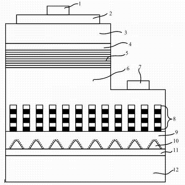
[0029] refer to figure 1 , the lowest layer of the device of the present invention is a sapphire substrate, the sapphire lining is low-temperature AlN buffer layer, the low-temperature AlN buffer layer is an undoped GaN nucleation layer, there is an air gap at the interface between the two, and the GaN nucleation layer is It is an n-type GaN buffer layer, and the interface between the two is DBR (SiO 2 / SiN 4 ) Multi-layer dielectric layer film structure, n-type GaN buffer layer is In x Ga 1-x N / Al y Ga l-y A multi-quantum well active region composed of N, a p-type AlGaN cladding layer on the multi-quantum well active region, and a p-type GaN contact layer on the cladding layer.

[0030] The fabrication of the device of the present invention includes two steps of material growth and device fabrication.

[0031] refer to figure 1 , the m...


PUM


Abstract

The invention discloses a manufacturing method for an InGaN/AlGaN-based near ultraviolet LED device. The device is mainly characterized in that: technologies including an embedded tapered air clearance structure and a patterning built-in DBR and the like are employed in a substructure of the device; the patterning built-in DBR is capable of blocking extension of threading dislocation, thereby substantially reducing a density of extended dislocation in an epitaxial layer and improving a crystal quality of an epitaxial film; meanwhile, because the structure of the DBR reflecting layer especially has a property of high reflectivity and an air clearance structure is especially designed on the bottom, reflection at many times and scattering on an upper surface can be carried out on lights emitted to a substrate, so that a light extraction efficiency of the LED can be substantially enhanced.

Description

technical field [0001] The invention belongs to the field of optoelectronic technology, and relates to material science and semiconductor devices, especially a near-ultraviolet LED device, which can be used in transportation, display, medicine, lighting, etc., but the most important application is in white light lighting. Background technique [0002] Near-ultraviolet LEDs refer to LEDs whose emission wavelength is in the range of 355-405nm. At present, GaN, the most widely used and most potential material in the research and production of LEDs, has a band gap of 3.4eV and a corresponding emission wavelength of 365nm, which is just in the near-ultraviolet range. Therefore, GaN is generally used in near-ultraviolet LEDs. N-type and p-type cladding layers. [0003] In recent years, GaN, InGaN, and AlGaN materials have been used to develop high-performance optical devices such as blue, green, and ultraviolet LEDs and lasers. This kind of nitride LED is widely used in mercury-...

Claims


Application Information

Patent Timeline
IPC IPC(8): H01L33/10H01L33/00
Inventor 徐瑾王江波魏世祯刘榕
Owner HC SEMITEK CORP
Why Eureka
Try Eureka