Epitaxial growth of relaxed silicon germanium layers

a technology of silicon germanium and relaxed growth, applied in the direction of crystal growth process, polycrystalline material growth, chemically reactive gas growth, etc., can solve problems such as adversely affecting device operation

Active Publication Date: 2005-03-10
ASM IP HLDG BV
View PDF23 Cites 41 Cited by
  • Summary
  • Abstract
  • Description
  • Claims
  • Application Information

AI Technical Summary

Benefits of technology

[0007] In one embodiment of the present invention, a relaxed silicon germanium structure comprises a silicon buffer layer produced using a chemical vapor deposition process with an operational pressure greater than approximately 1 torr. The relaxed silicon germanium structure further comprises a silicon germanium layer deposited over the silicon buffer layer. The silicon germanium layer has less than about 107 threading dislocations per square centimeter.
[0008] In another embodiment of the present invention, a method of producing a relaxed silicon germanium structure comprises epitaxially depositing a silicon-containing layer using a chemical vapor deposition process with an operational pressure greater than approximately 1 torr. The method further comprises heteroepitaxially depositing a germanium-containing layer over the silicon-containing layer. The germanium-containing layer has a lattice constant that differs from a lattice constant of the silicon-containing layer. The germanium-containing layer has a surface roughness that is less than approximately 3 nm rms.
[

Problems solved by technology

Unfortunately, relaxation often accompanies vertically propagating

Method used


Image

  • Epitaxial growth of relaxed silicon germanium layers
  • Epitaxial growth of relaxed silicon germanium layers
  • Epitaxial growth of relaxed silicon germanium layers

Examples


Embodiment Construction

[0025] As used herein, the terms “single-crystal” and “epitaxial” are used to describe a predominantly large crystal structure that may have a tolerable number of faults therein. Crystallinity of a layer generally falls along a continuum from amorphous to polycrystalline to single-crystal, and therefore a crystal structure is often considered single-crystal or epitaxial notwithstanding a low density of faults. The term “epitaxy” refers to deposition where the deposited layer serves as an extension of the crystal structure of an underlying layer. “Heteroepitaxy” is a species of epitaxy in which the underlying layer and the overlying deposited layer are of different materials.

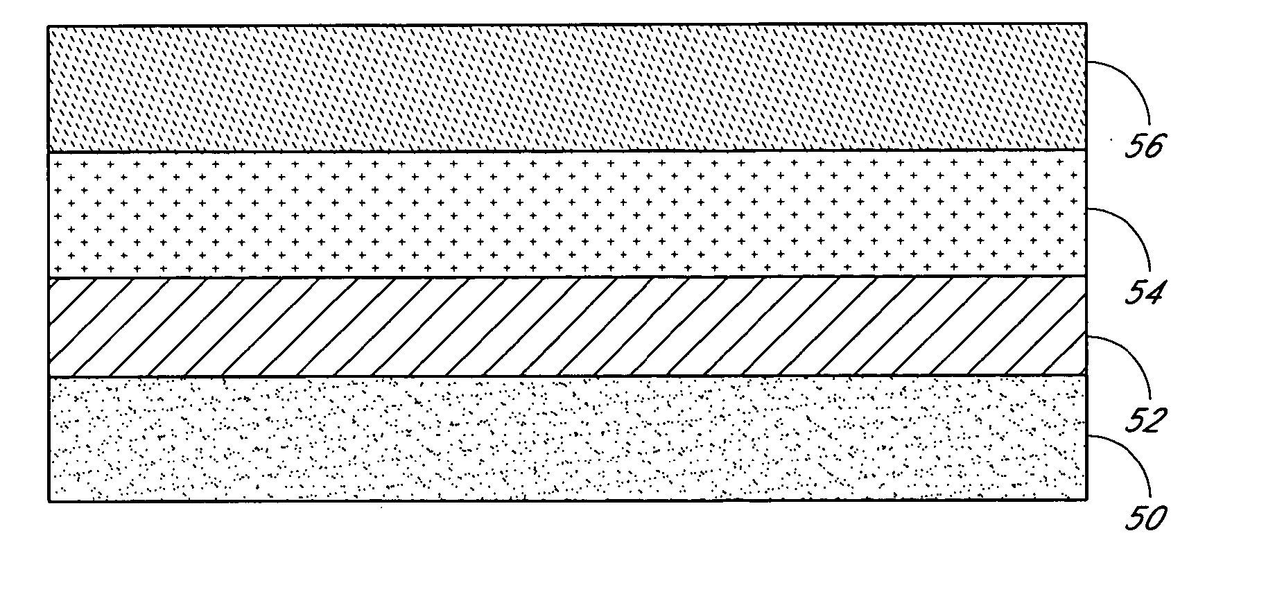
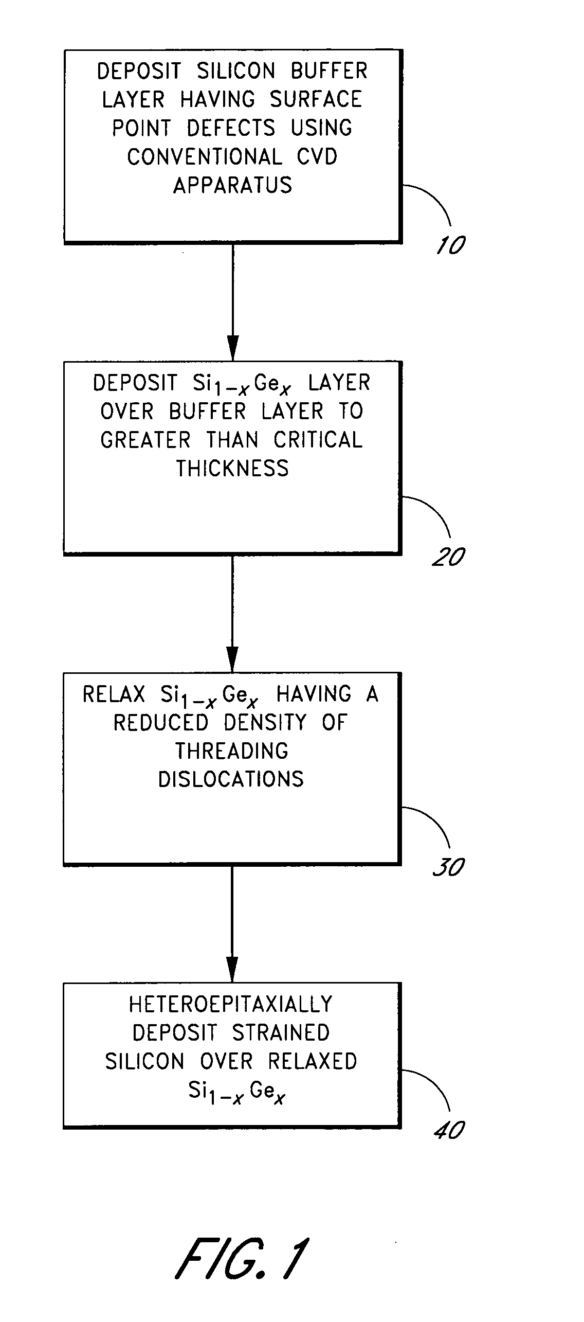
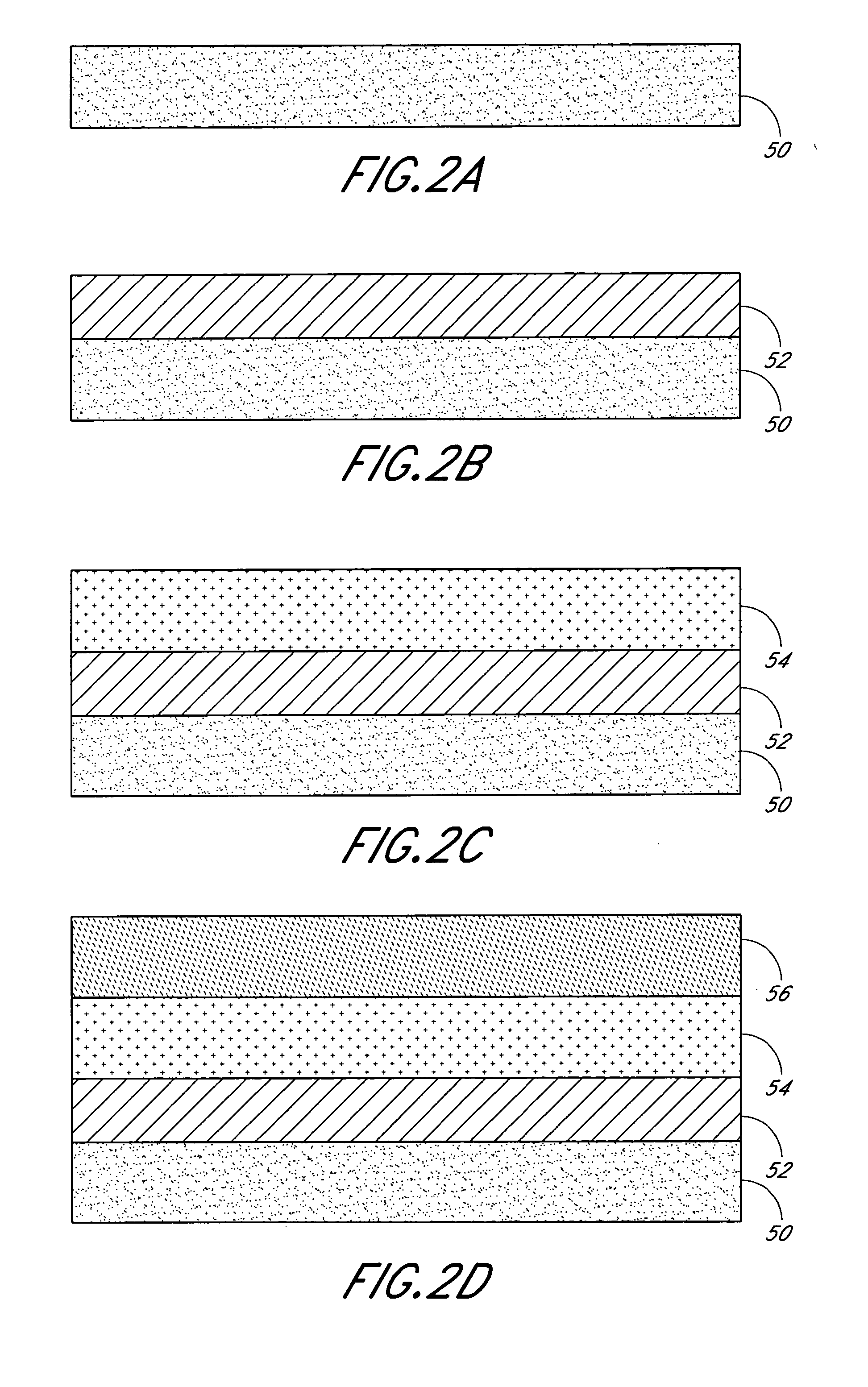
[0026] As described above, as the thickness of a strained silicon germanium layer increases beyond the critical thickness, defects in the crystal structure of the strained silicon germanium layer appear, thus leading to relaxation of the strained layer. Such defects can include threading dislocations. Generally,...


PUM


Abstract

A relaxed silicon germanium structure comprises a silicon buffer layer produced using a chemical vapor deposition process with an operational pressure greater than approximately 1 torr. The relaxed silicon germanium structure further comprises a silicon germanium layer deposited over the silicon buffer layer. The silicon germanium layer has less than about 107 threading dislocations per square centimeter. By depositing the silicon buffer layer at a reduced deposition rate, the overlying silicon germanium layer can be provided with a “crosshatch free” surface.

Description

PRIORITY APPLICATION [0001] This application claims the benefit of U.S. Provisional Patent Application 60 / 491,029, filed Jul. 30, 2003, the entire disclosure of which is hereby incorporated by reference herein. [0002] This application is also related to U.S. Provisional Patent Application 60 / 455,226 (filed Mar. 13, 2003), U.S. Provisional Patent Application 60 / 470,584 (filed May 14, 2003), and U.S. patent application Ser. No. 10 / 800,390 (filed Mar. 12, 2004). The entire disclosure of these three related applications are also hereby incorporated by reference herein. FIELD OF THE INVENTION [0003] The present invention relates generally to the formation of silicon germanium layers in a chemical vapor deposition process, and relates more specifically to epitaxial growth of relaxed silicon germanium layers. BACKGROUND OF THE INVENTION [0004] Strained semiconductor materials advantageously provide improved electrical carrier mobility properties as compared to relaxed semiconductor materia...

Claims


Application Information

Patent Timeline
IPC IPC(8): C30B25/02C30B29/06C30B29/52H01LH01L21/20H01L21/205H01L29/732
CPCC30B25/02C30B29/06C30B29/52H01L21/0262H01L21/02494H01L21/02502H01L21/02532H01L21/0245H01L21/20
Inventor ARENA, CHANTALTOMASINI, PIERRECODY, NYLESBAUER, MATTHIAS
Owner ASM IP HLDG BV
Why Eureka
Try Eureka