Hexadecagonal routing

a technology of hexadecagon and routing, applied in the field of microelectronic integrated circuits, can solve the problems of increasing the number of transistors, increasing the time required for data communication, and requiring more functionality

Inactive Publication Date: 2003-07-08
AVAGO TECH INT SALES PTE LTD
View PDF5 Cites 204 Cited by
  • Summary
  • Abstract
  • Description
  • Claims
  • Application Information

AI Technical Summary

Problems solved by technology

However, the demand for more functionality will require an increase in the number of transistors that need to be integrated on a chip.
In the past, the time required for data communication was typically insignificant compared to the time required for computation, and could be neglected.
Now, the interconnection delays are on the order of gate delays and as a result, have become significant and can no longer be ignored.
Interconnect delays are an increasing percentage of path delay.
When two wires in the same metal layer run parallel to each other, parasitic capacitances may be significant and "crosstalk" may occur between signals on those wires.
This has resulted in unsatisfactory capacitance and "crosstalk" in many instances.
Significant performance degradation may result.
It is an extremely tedious and an error-prone process because of the tight tolerance requirements, the complexity of the design rules, and the minuteness of the individual components.
Achievement of this goal is restricted using conventional rectilinear routing because diagonal connections are not possible.
Another drawback of conventional rectilinear interconnect routing is its sensitivity to parasitic capacitance.
Since many conductors run in the same direction in parallel with each other, adjacent conductors form parasitic capacitances that can create signal crosstalk and other undesirable effects.
Achievement of this goal is restricted using conventional rectilinear routing because diagonal connections are not possible.
Another drawback of conventional rectilinear interconnect routing is its sensitivity to parasitic capacitance.
Since many conductors run in the same direction in parallel with each other, adjacent conductors form parasitic capacitances that can create signal crosstalk and other undesirable effect.
But, as discussed above, conventional rectilinear routing suffers from many problems.

Method used


Image

  • Hexadecagonal routing
  • Hexadecagonal routing
  • Hexadecagonal routing

Examples


Embodiment Construction

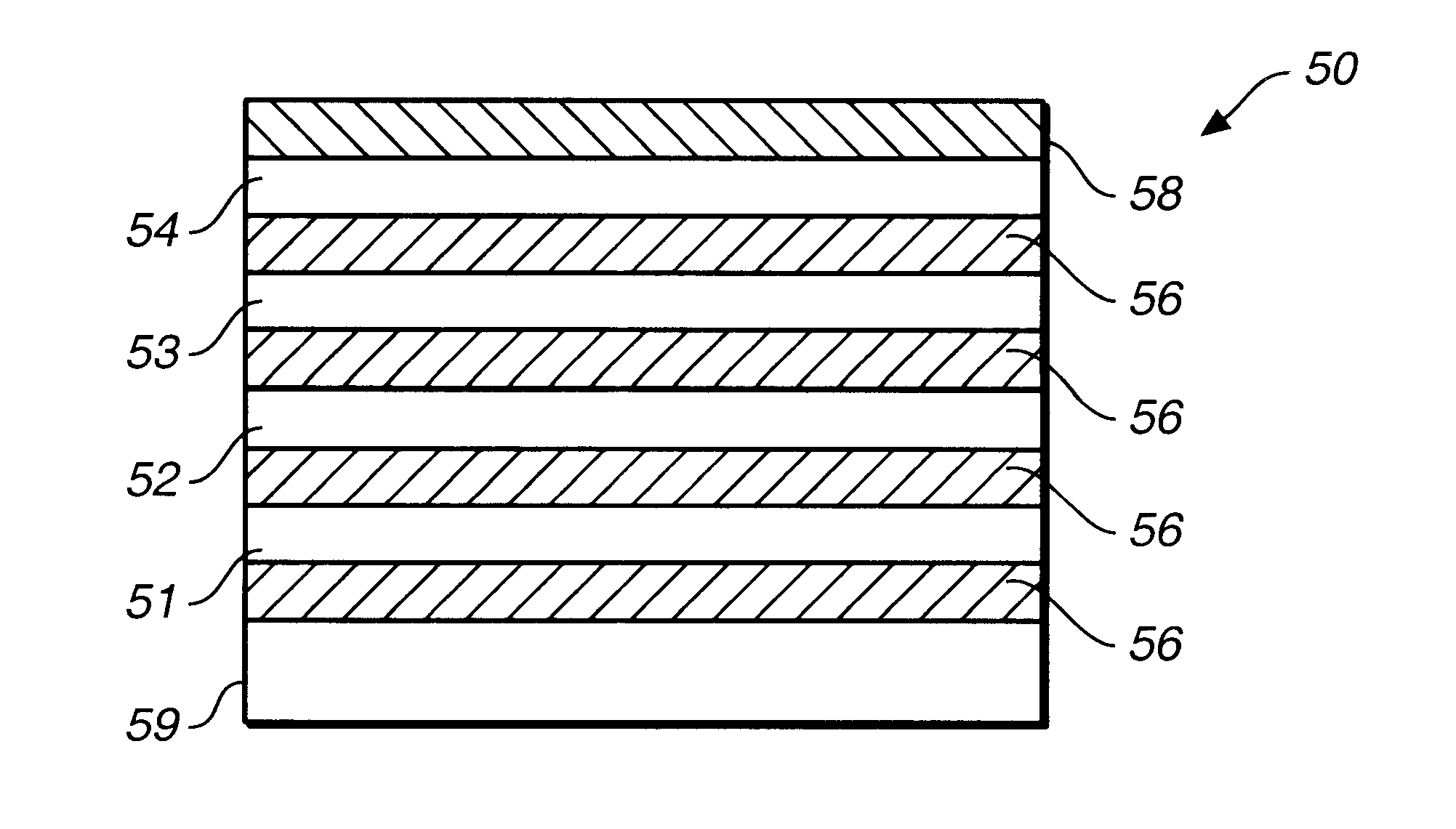
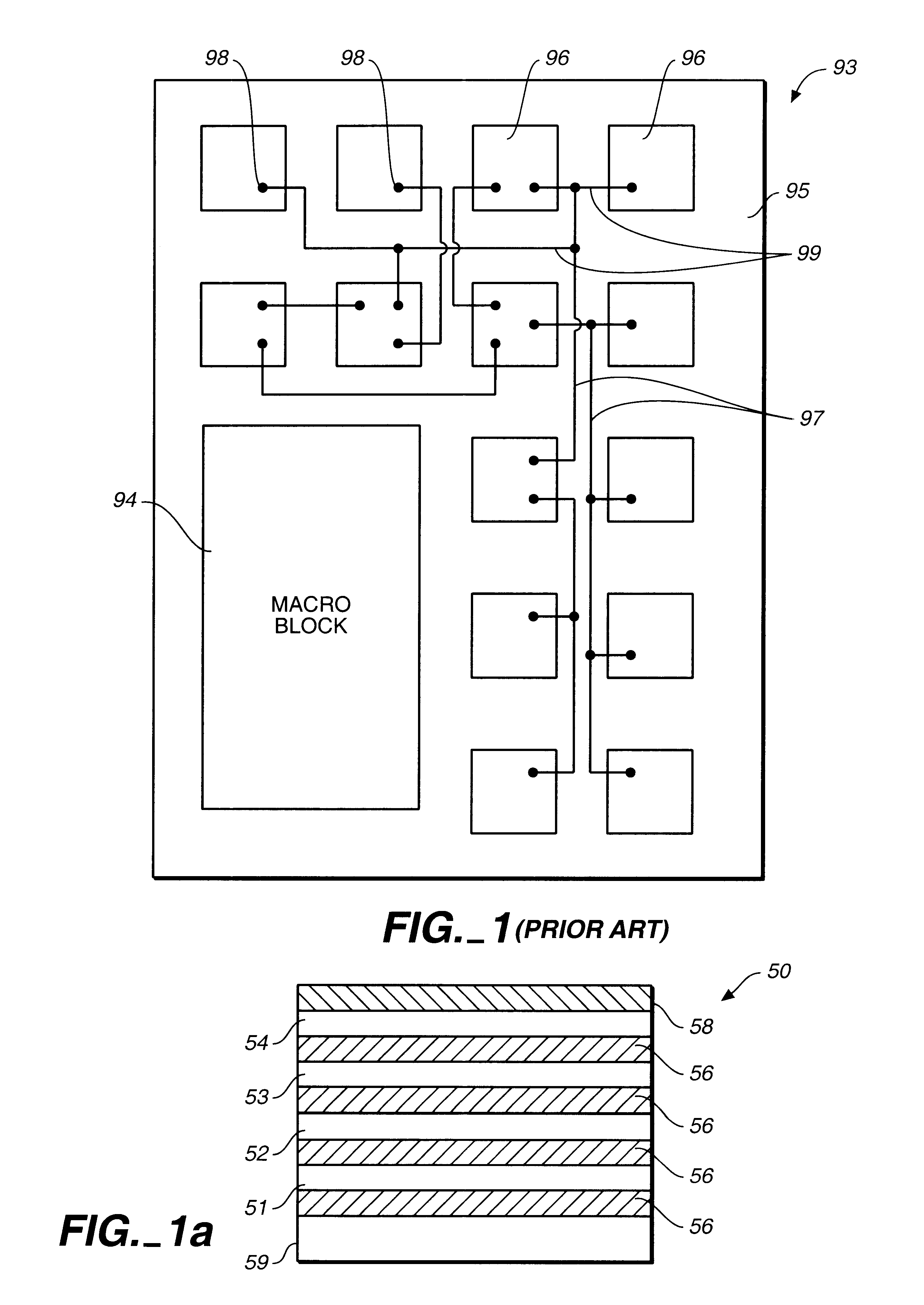
FIG. 1a provides a simplified cross-sectional view of a typical integrated circuit chip (or die) 50. As shown in FIG. 1a, chip 50 includes a semiconductor substrate 59, metal layers 51 to 54, electrically insulating layers 56, and passivation layer 58. Semiconductor substrate 59, which is typically polysilicon, is used for forming the transistors and other electronic devices.

Metal layers 51 to 54 may be formed from any of a variety of materials including aluminum, copper or an electrically conductive alloy. Between metal layers 51 and 52, 52 and 53, and 53 and 54, and between metal layers 51 and substrate 59 is an electrically insulating layer 56, which typically is formed as an oxide film. Connections between any of metal layers 51 to 54 and semiconductor substrate 59 are made using interlayer holes called vias. Passivation layer 58 functions to prevent the deterioration of the electrical properties of the die caused by water, ions and other external contaminants, and typically is ...


PUM


Abstract

Cell terminals in an integrated circuit is interconnected by using multiple layers of conductors that are routed both orthogonally and non-orthogonally to each other. Non-orthogonally routed conductors have slopes that are ratios of non-zero integers which approximate ceratin predetermined angles. The integers in the ratios are chosen from integers generated by sequence equations. The conductors are routed by following grid lines in a grid system comprising both orthogonal grid lines and non-orthogonal grid lines having slopes generated by the sequence equations. Ratios of integers are used to approximate certain angles so that the conductors would intersect the cell terminals located on the fundamental grid intersection points. The conductors in different metal layers form different angles with other conductors in other metal layers based on the slopes of the conductors.

Description

1. Field of the InventionThe present invention generally relates to the art of microelectronic integrated circuits. In particular, the present invention relates to the art of using multiple layers of metals to route the cells in integrated circuits.2. Description of the Prior ArtThe fabrication of semiconductor devices has progressed significantly over the last four decades. Some semiconductor chips incorporate over a million transistors. However, the demand for more functionality will require an increase in the number of transistors that need to be integrated on a chip. This will require shrinking the area required to fabricate interconnected transistors or will require larger die sizes, or both. As the feature size decreases and the area required to fabricate transistors decreases, the resulting increased density of devices will require an increasing number of interconnections within a chip, or interconnections between chips in a multi-chip design.Transistors or gates typically ma...

Claims


Application Information

Patent Timeline
Patent Type & Authority Patents(United States)
IPC IPC(8): G06F17/50H01L23/52H01L23/528
CPCG06F17/5077H01L23/528H01L2924/0002H01L2924/00G06F30/394
Inventor SHIVELY, JOHN
Owner AVAGO TECH INT SALES PTE LTD
Why Eureka
Try Eureka