Printed wiring board structure with z-axis interconnections

a wiring board and z-axis interconnection technology, applied in the direction of printed element electric connection formation, etching metal masks, lighting and heating apparatus, etc., can solve the problems of increasing the cost of manufacture by a large amount, and the processing apparatus is extremely complex and requires the utilization of expensive robotics

Inactive Publication Date: 2003-07-15
INT BUSINESS MASCH CORP
View PDF7 Cites 21 Cited by
  • Summary
  • Abstract
  • Description
  • Claims
  • Application Information

AI Technical Summary

Benefits of technology

It is to be understood that the present invention offers the flexibility of creating many different interlayer connections and resultant structures that will become readily apparent to those skilled in the art.

Problems solved by technology

Higher yields will result from processing the individual layers within the capabilities and physical limitations.
This entails a relatively complex manufacturing procedure, which although providing for appropriate electrical interconnects intermediate the various layers of the multilayer semiconductor device, requires extensive processing which appreciably increases the cost of manufacture.
This construction is complex and, resultingly, difficult to align during manufacture and assembly, so as to be conducive to extensive manufacturing costs in forming the multilayer or stacked electric circuit arrangement.
Again, although this provides for a generally satisfactory method of registering and stacking layers of a thin laminate forming a semiconductor structure, the processing apparatus is extremely complex in requiring the utilization of expensive robotics in order to provide for accurately aligned positioning of the various electric components, interconnects and layers.

Method used


Image

  • Printed wiring board structure with z-axis interconnections
  • Printed wiring board structure with z-axis interconnections
  • Printed wiring board structure with z-axis interconnections

Examples


Embodiment Construction

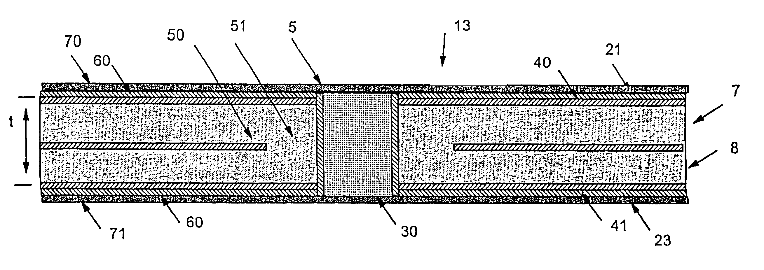
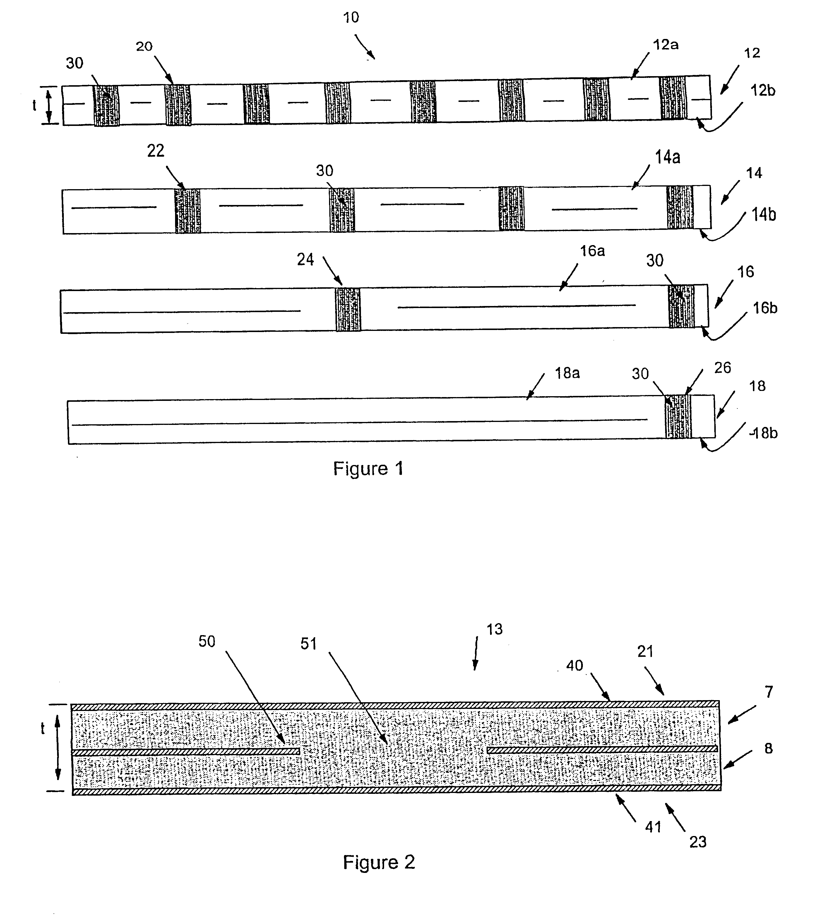
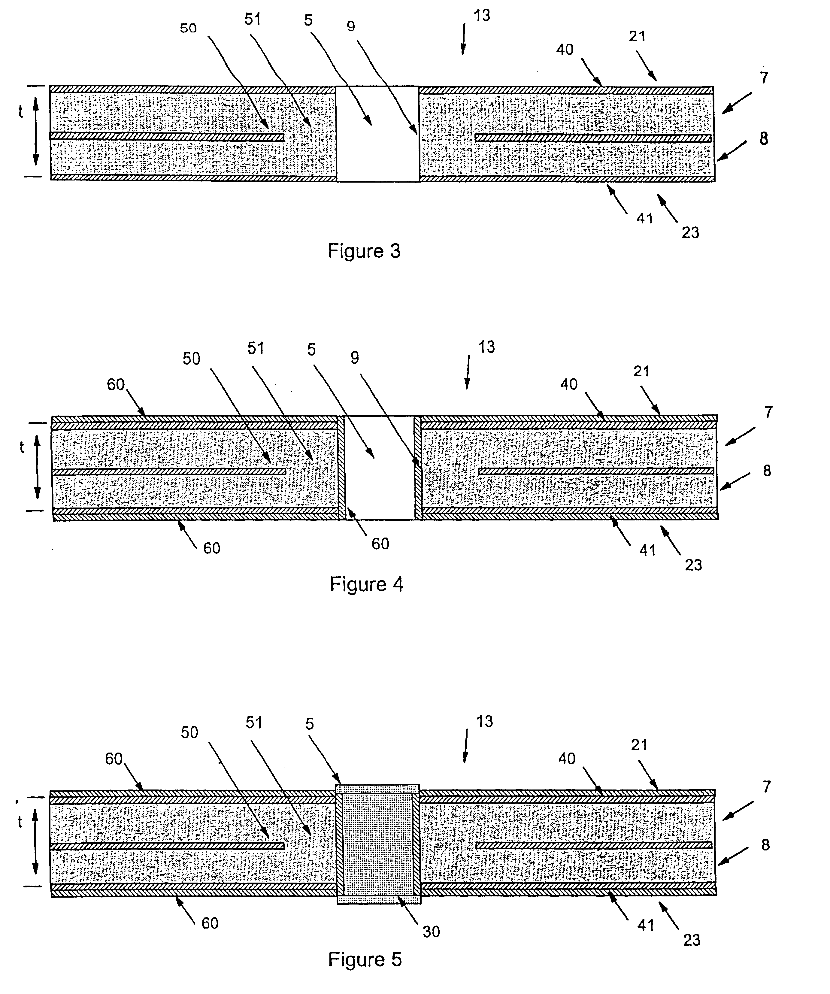
Referring now in detail to the drawings, and more specifically to FIG. 1, for the formation of a multilayer printed wiring board 10, there is illustrated a plurality of separate layers 12, 14, 16 and 18, in this instance, by way of example, consisting of a total of four layers. Each of the layers is constituted of an essentially dielectric material, such as an organic substrate, as is well known, and may be equipped on their respective opposite surfaces 12a, 12b; 14a, 14b; 16a, 16b; and 18a, 18b with suitable circuitized plating and / or wiring. This may be selectively applied either with or without a mask, as is well known in the technology. Each of the layers 12, 14, 16 and 18 may possess a thickness "t" of preferably, but not necessarily, within the range of about 20-100 mils, depending upon the sizes of holes or vias to be formed therein.

Formed respectively in each of the layers 12, 14, 16, 18 prior to lamination thereof, are a plurality of through extending holes or vias 20, 22, ...


PUM


Abstract

A structure of and method for producing a multilayer printed or wiring circuit board, and more particularly a method producing so-called z-axis or multilayer electrical interconnections in a hierarchial wiring structure in order to be able to provide for an increase in the number of inputs and outputs (I / O) in comparison with a standard printed wiring board (PWB) arrangement, and a printed wiring board produced by the method.

Description

1. Field of the InventionThe present invention relates to a method for producing a multilayer printed or wiring circuit board, and more particularly pertains to a method producing so-called z-axis or multilayer electrical interconnections in a hierarchial wiring structure in order to be able to provide for an increase in the number of inputs and outputs (I / O) in comparison with a standard printed wiring board (PWB) arrangement.As the complexity of printed wiring boards increases, the need to increase the wiring density on each inner layer becomes more critical. Many complex PWB's currently have wiring grids of 1.0 mm (40 mil). Future applications will drive the need to extend that wiring grid to 0.50 mm or less. This drives the need for smaller line widths and line spacings, as well as smaller wiring vias on the inner layers and external wiring surfaces circuit board as the wiring grid (pitch) decreases. Consequently, smaller via holes must be drilled throughout the length of the PW...

Claims


Application Information

Patent Timeline
Patent Type & Authority Patents(United States)
IPC IPC(8): H05K3/46H05K3/40H05K1/11
CPCH05K3/462H05K1/115H05K3/4069H05K2201/0347H05K2201/0352H05K2201/09536H05K2201/0959H05K2201/096H05K2203/0554
Inventor JONES, GERALD W.LAUFFER, JOHN M.MARKOVICH, VOYA R.MILLER, THOMAS R.PAOLETTI, JAMES P.PAPATHOMAS, KONSTANTINOS I.STACK, JAMES R.
Owner INT BUSINESS MASCH CORP
Why Eureka
Try Eureka