

Semiconductor device testing method and system employing trace data
a technology of a semiconductor device and a trace data, applied in the direction of measurement devices, electronic circuit testing, instruments, etc., can solve the problems of affecting the performance of the device, the failure to solve the problem of kgd malfunctioning for such a specific pattern combination, and the loss of significant amoun
- Summary
- Abstract
- Description
- Claims
- Application Information
AI Technical Summary
Problems solved by technology
Method used
Image

Examples
Embodiment Construction
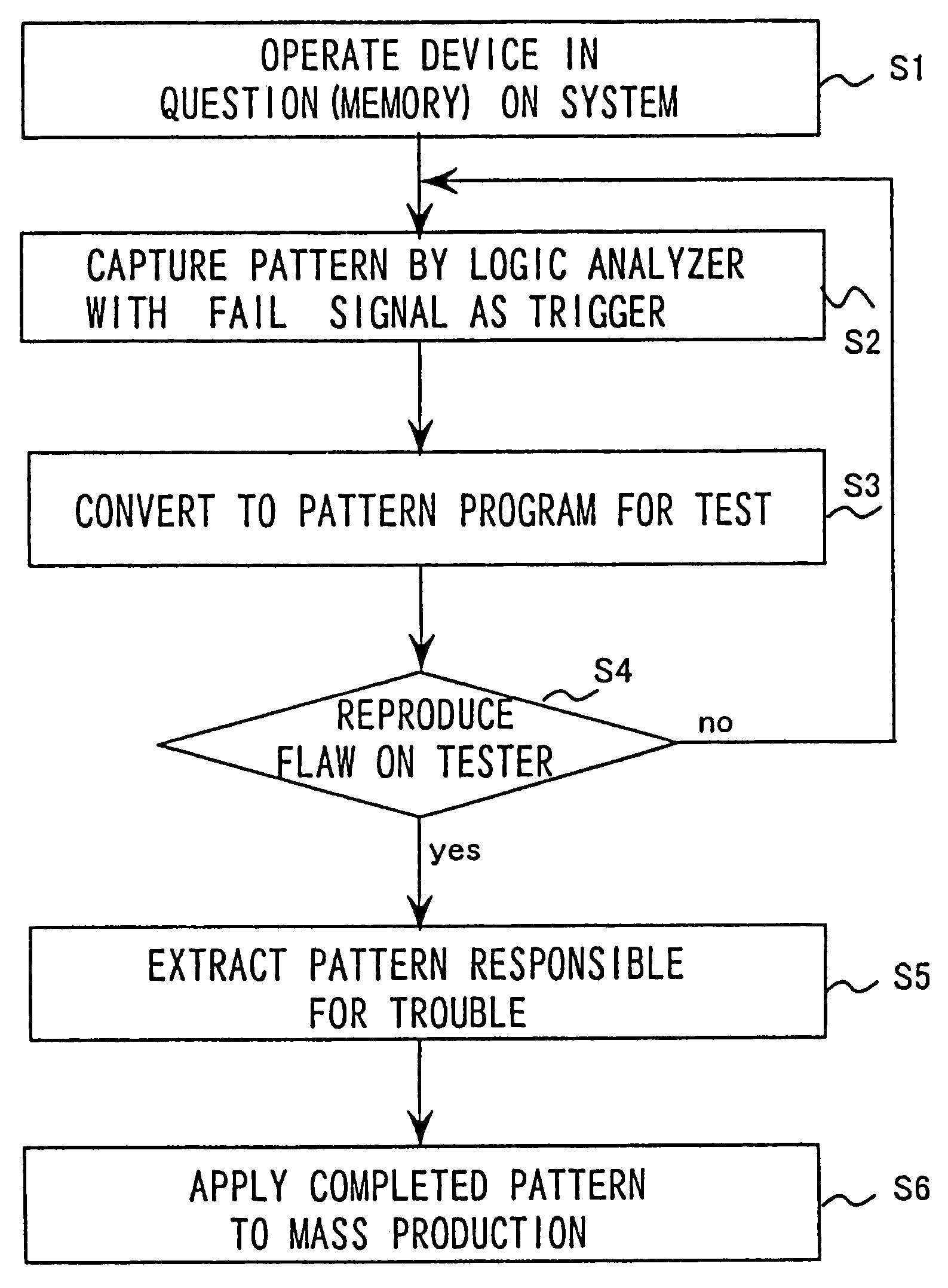
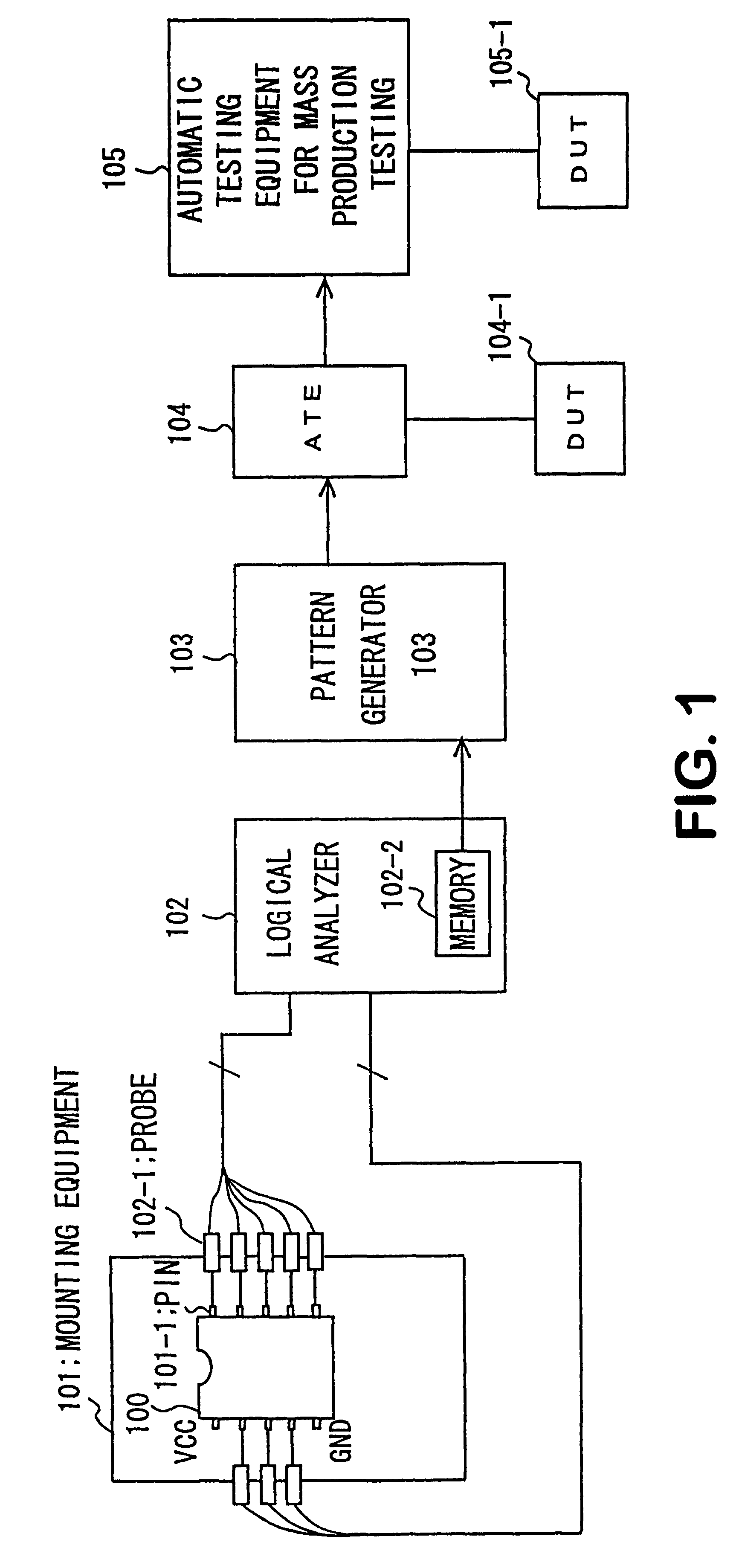
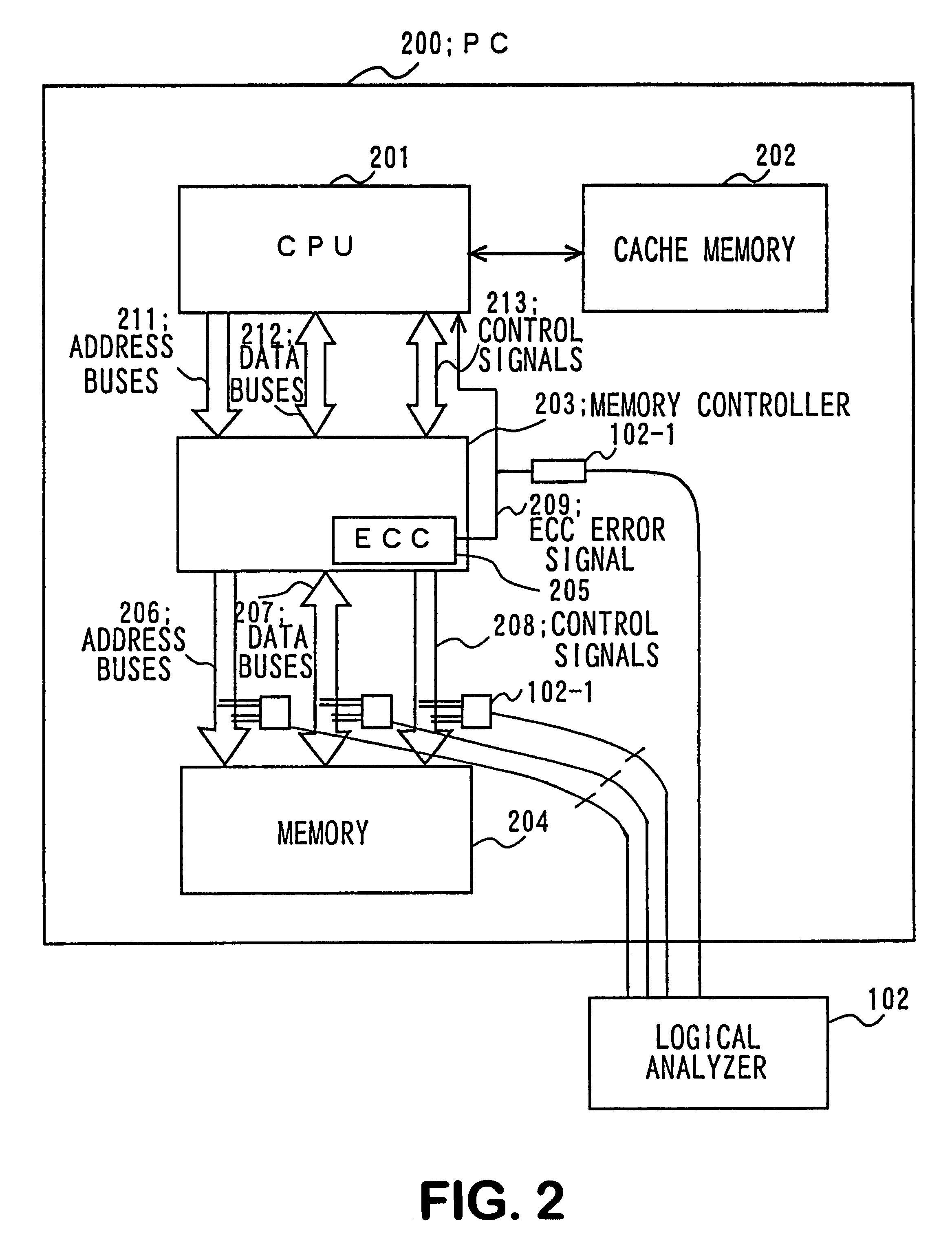
Preferred embodiments of the present invention are now explained. The system of the present invention includes a device for acquiring signal waveform data 102 for a time period beginning from a first time point going back retrogressive as from the time of occurrence of a malfunction of the semiconductor device and running until a second time point inclusive of a malfunctioning time of the semiconductor device, as signal waveform data at a preset group of terminals of a (first) semiconductor device, and a device for generating a test pattern usable in automatic testing equipment 103 for testing a semiconductor device as a device under test, from the acquired signal waveform data. The pattern generating device 103 generates and outputs a test pattern which is the data for the malfunctioning time that has been changed to normal data and, using a mass production test generated in the automatic testing equipment 105, conducts a mass production test on a semiconductor device which is of t...
PUM
 Abstract
Description
Claims
Application Information