
Non-volatile memory and method for fabricating the same

Inactive Publication Date: 2003-10-07
LAPIS SEMICON CO LTD
View PDF2 Cites 15 Cited by
  • Summary
  • Abstract
  • Description
  • Claims
  • Application Information

AI Technical Summary

Benefits of technology

Accordingly, an object of the present invention is to provide a non-volatile memory of which the integration can be improved easily without lowering the characteristics and reliability thereof.
Another object of the present invention is to provide a method for fabricating a non-volatile memory in which the integration of the memory can be improved easily without lowering the characteristics and reliability thereof.

Problems solved by technology

Therefore, it is difficult to improve integration of the memory.

Method used


Image

  • Non-volatile memory and method for fabricating the same
  • Non-volatile memory and method for fabricating the same
  • Non-volatile memory and method for fabricating the same

Examples


first preferred embodiment

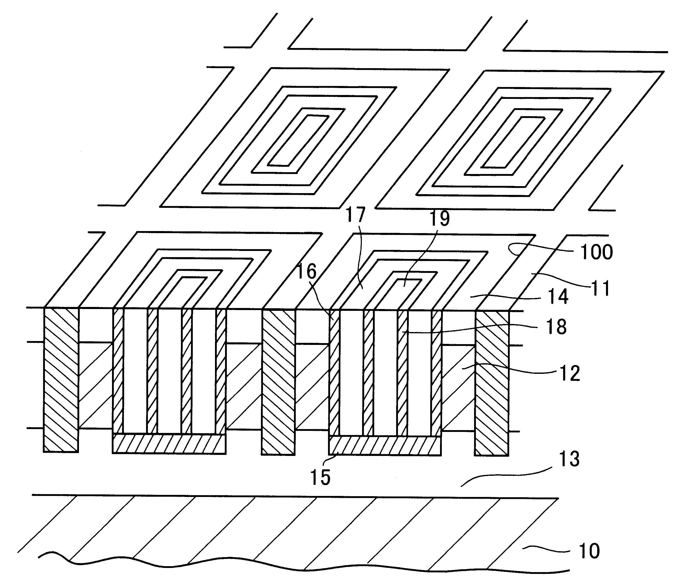
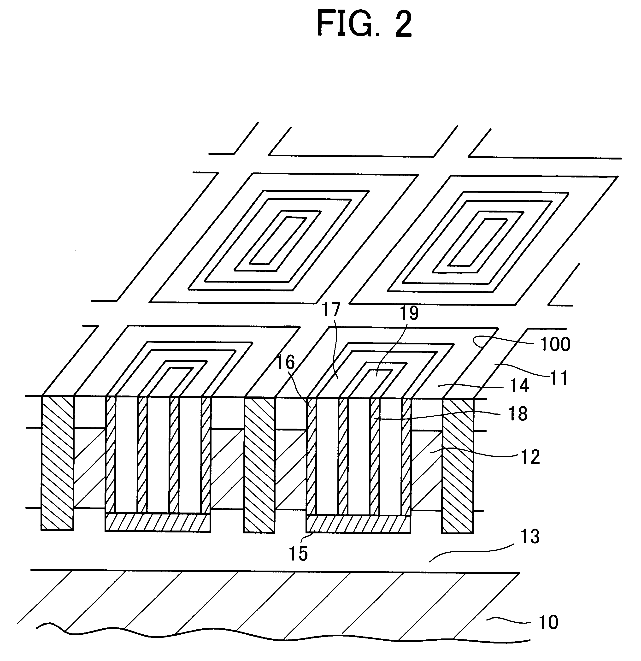
FIG. 2 shows a part of a non-volatile memory according to a first preferred embodiment of the present invention. The non-volatile memory includes a p-type of silicon substrate 10, on which cell-isolating insulation layers 11 are formed in matrix to separate a plurality of memory cells. Each region or cavity 100 segmented by the cell-isolating insulation layers 11 is designed to have inside walls provided with active regions 12, which is a part of the p-type silicon substrate 10. The memory further includes a common source region 13 formed on the silicon substrate 10 under the active regions 12. In the common source region 13, high density n+ ions are implanted. A drain region 14 is formed on the active regions 12. In the drain region 14, n-ions are implanted. The common source region 13, active regions 12 and drain region 14 form a channel for a transistor, which is used for storing data.

A gate insulating layer 16 is formed on an inside surface of the active regions 12, which is sha...

second preferred embodiment

FIG. 4 shows a non-volatile memory according to a second preferred embodiment of the present invention, in which the same or corresponding elements or components to those in the first preferred embodiment, shown in FIG. 2, are represented by the same reference symbols. The differences from the non-volatile memory according to the first preferred embodiment, shown in FIG. 2, is the structure of floating gate electrode and control gate electrode.

A non-volatile memory according to the second preferred embodiment includes a p-type of silicon substrate 10, on which cell-isolating insulation layers 11 are formed in matrix to separate a plurality of memory cells. Each region segmented by the cell-isolating insulation layers 11 is designed to have inside walls provided with active regions 12, which is a part of the p-type silicon substrate 10. The memory further includes a common source region 13 formed on the silicon substrate 10 under the active regions 12. In the common source region 13,...

third preferred embodiment

FIG. 5 shows a non-volatile memory according to a third preferred embodiment of the present invention. The non-volatile memory includes a p-type silicon substrate 20 and pillar shape of active regions 21 formed on the silicon substrate 20. The active regions 21 are arranged in the orthogonal two directions with predetermined intervals. The non-volatile memory further includes a common source region 22 formed under the active regions 21 on the silicon substrate 20. The common source region 22 is formed by implanting n+ ions. A drain region 23 is formed on the active region 21 by implanting n-ions.

An insulating layer 24 is formed on the surface of the silicon substrate 20 except the active regions 21. The active region 21 is provided at an outer side surface with a gate insulating layer 25. The gate insulating layer 25 is arranged to surround the active region 21. A floating gate electrode is formed on a side surface of the gate insulating layer 25. An inter-gate insulating layer 27 i...


PUM


Abstract

A non-volatile memory includes a substrate: a floating gate electrode and a control gate electrode formed on the substrate; and an active layer formed around the control gate and the floating gate. The active layer has source and drain and a channel layer between the source and drain.

Description

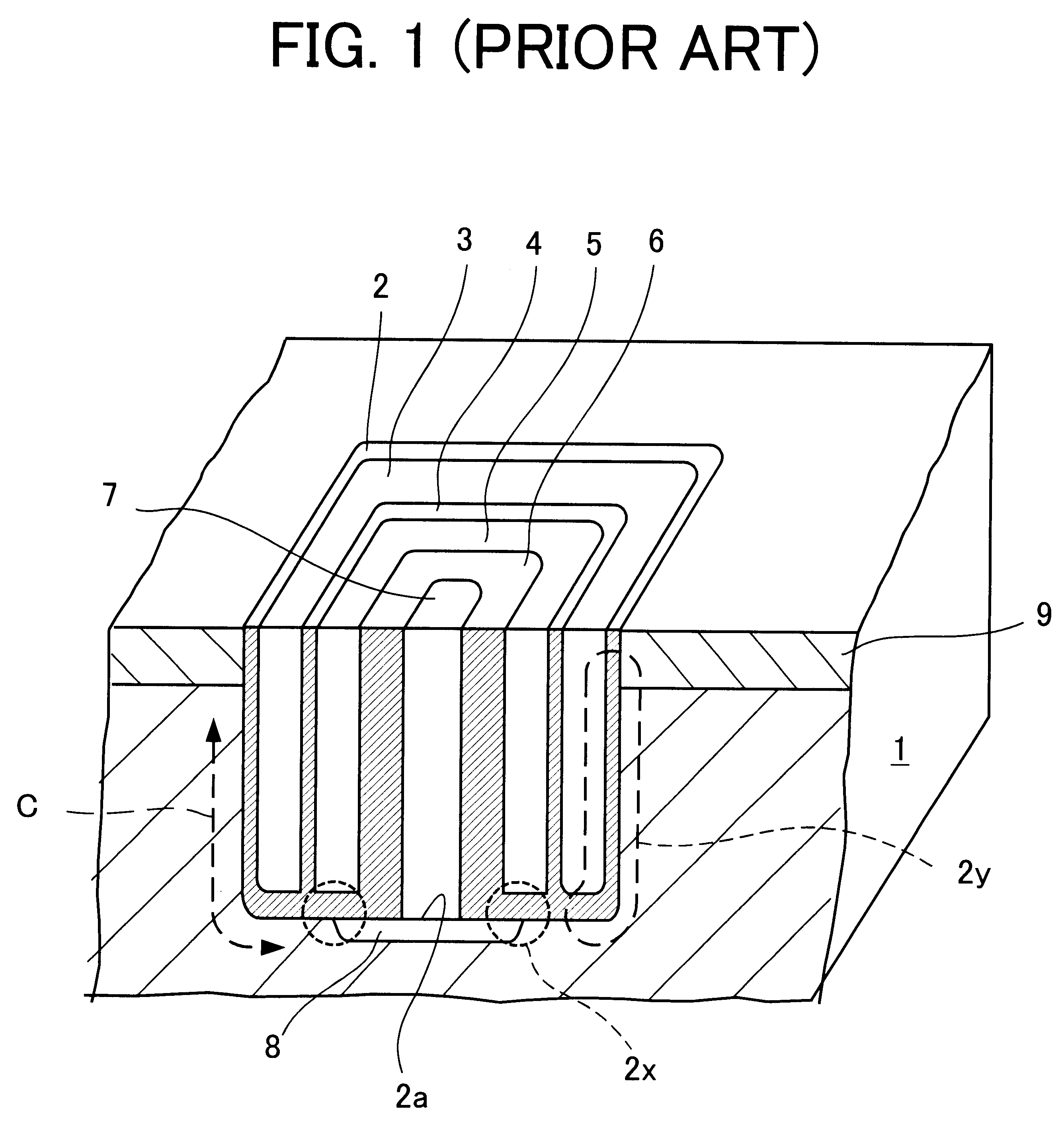
This application claims the priority of Application No. 2000-066703, filed Mar. 10, 2000 in Japan, the subject matter of which is incorporated herein by reference.The present invention relates to a non-volatile memory such as an EEPROM (Electrically Erasable and Programmable Read Only Memory) and a flash memory. The present invention also relates to a method for fabricating a non-volatile memory.A conventional non-volatile memory is described, for example, in a Japanese Laying Open Publication H05-315622.FIG. 1 shows a conventional non-volatile memory shown in the above-described Japanese publication. The non-volatile memory includes a p-type silicon substrate 1 having a square shape of cavity (groove) therein. The cavity is provided at a side wall and a bottom surface with an insulating layer 2 having a pass-through hole 2a at the center. On the inside wall of the insulating layer 2, a control gate electrode 3, an inter-gate insulating layer 4, a floating gate electrode 5 and an in...

Claims


Application Information

Patent Timeline
IPC IPC(8): H01L21/8247H01L21/70H01L29/66H01L27/115H01L29/788H01L29/792
CPCH01L27/115H01L29/7885H01L27/11556H10B41/27H10B69/00
Inventor UCHIYAMA, AKIRA
Owner LAPIS SEMICON CO LTD
Learn More