Surface emitting semiconductor laser and method of manufacturing the same

a semiconductor laser and surface technology, applied in semiconductor lasers, laser details, optical resonator shape and construction, etc., can solve the problem of difficult to control the shape of the inner edge to be closer to a true circl

Inactive Publication Date: 2003-10-07
SEIKO EPSON CORP
View PDF2 Cites 11 Cited by
  • Summary
  • Abstract
  • Description
  • Claims
  • Application Information

AI Technical Summary

Benefits of technology

By means of this construction, by forming the strain application portion in the pillar-form semiconductor deposition, the polarization of the laser light can be controlled.

Problems solved by technology

However, as described above, since the current constriction layer is formed by oxidation of the current constriction layer formation layer from the lateral surface, because of the oxidation conditions it is difficult to control the shape of the inner edge to be closer to a true circle.

Method used


Image

  • Surface emitting semiconductor laser and method of manufacturing the same
  • Surface emitting semiconductor laser and method of manufacturing the same
  • Surface emitting semiconductor laser and method of manufacturing the same

Examples


first embodiment

A. Device Manufacturing Process

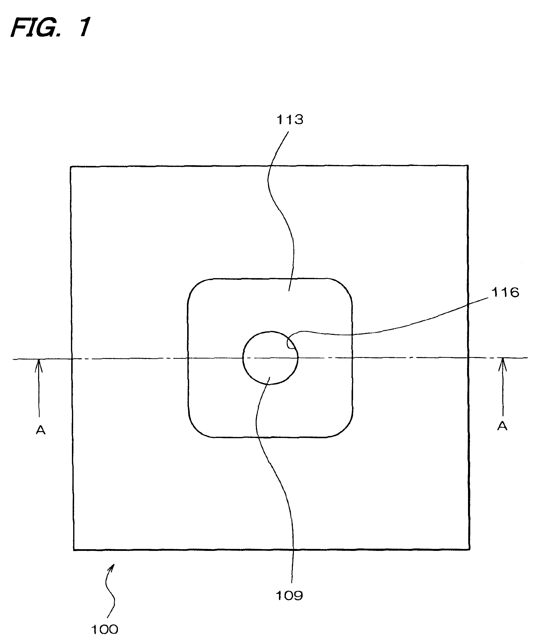
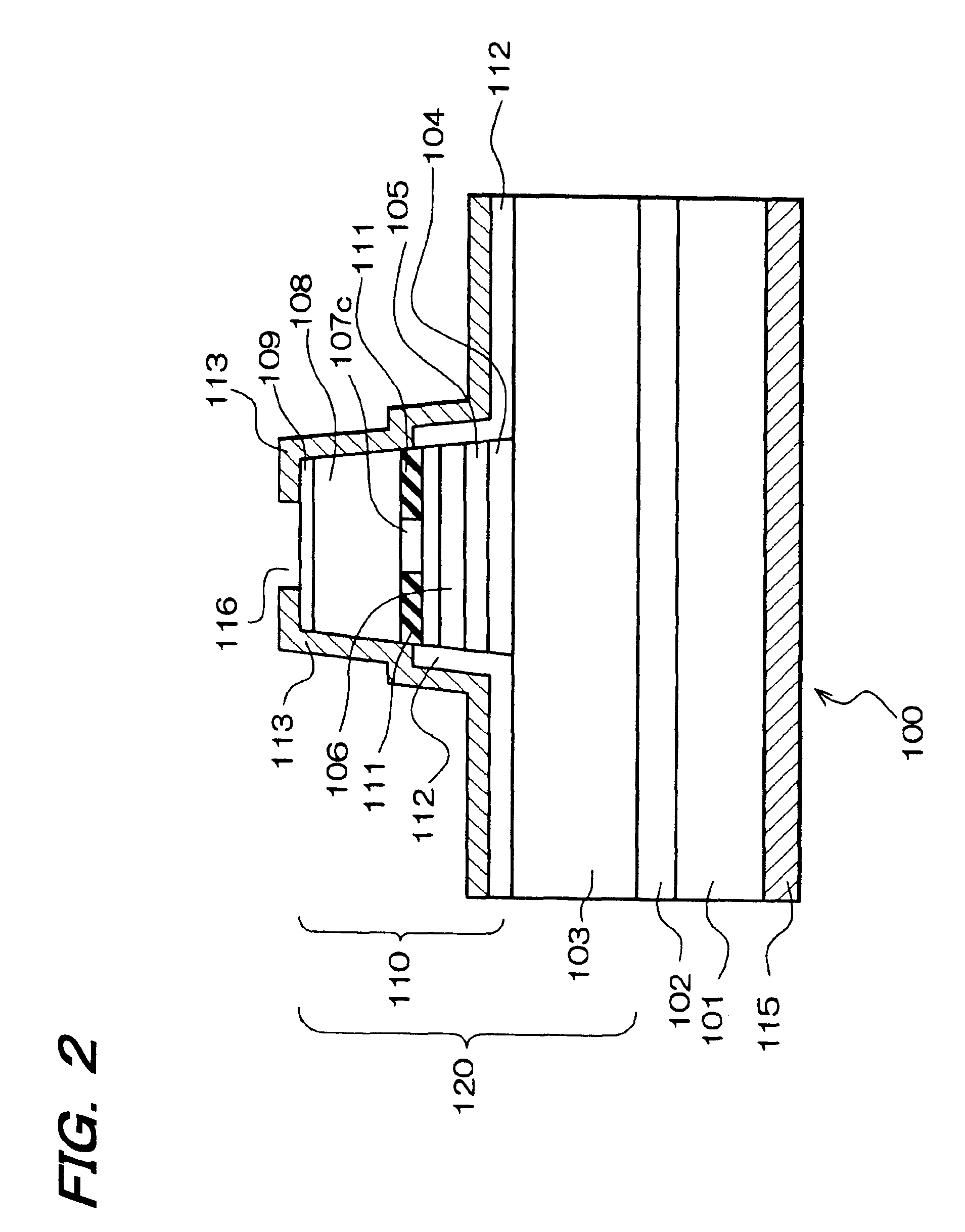
First, the method of manufacturing the first embodiment of the surface emitting semiconductor laser (referred to hereinafter as "surface emitting laser") 100 of the present invention is described with reference to FIGS. 4 to 7. FIGS. 4 to 6 are sectional views, schematically showing the manufacturing process of a surface emitting laser 100 of this embodiment. FIG. 7 schematically shows a cross-section of a pillar portion 110 formed in the manufacturing process of the first embodiment of the surface emitting laser 100 shown in FIG. 5, in the plane including a current constriction layer formation layer 107a.

The method of manufacturing the surface emitting laser 100 of this embodiment comprises principally the following steps (a) to (c).

Step (a) is principally a step of laminating on a semiconductor substrate 101 having Miller indices (100), semiconductor deposition layers 150 including a current constriction layer formation layer 107a.

Step (b) is princip...

second embodiment

the surface emitting laser 200 provides the same operation as the first embodiment of the surface emitting laser 100, and further the same effect and benefit. Description is therefore omitted here.

Third Embodiment

A. Device construction

FIG. 9 is a sectional view, schematically showing a surface emitting laser 300 of the third embodiment of the present invention.

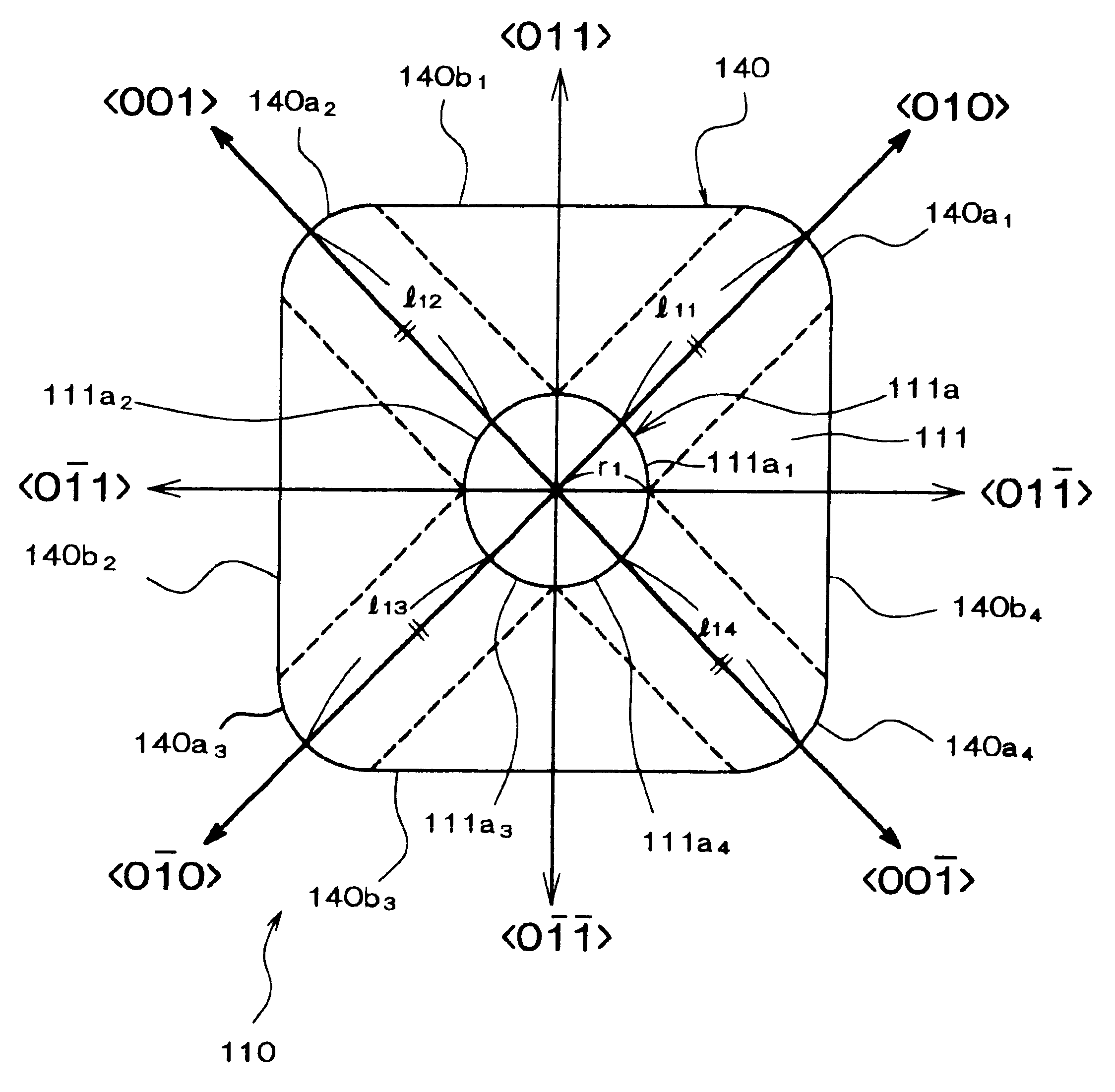
The third embodiment of the surface emitting laser 300 has substantially the same construction as the second embodiment of the surface emitting laser 200, except that on a pillar portion 310 is formed a strain application portion 330 which generates a strain in the active layer (not shown in the drawings). The shape of the periphery 340 of the pillar portion 310, like the pillar portion 210, is constituted by arc-shaped portions 340a.sub.1, 340a.sub.2, 340a.sub.3, and 340a.sub.4, and curved lines 340b.sub.1, 340b.sub.2, 340b.sub.3, and 340b.sub.4 joining adjacent of the arc-shaped portions. Further, the distance 1.sub.31 betwe...

third embodiment

the surface emitting laser 300 provides substantially the same effect and benefit as the effect and benefit of the first and second embodiments of the surface emitting laser 100 and 200, and further provides the following benefit.

In the third embodiment of the surface emitting laser 300, by virtue of the strain application portion 330 being formed on the pillar portion 310, laser light emission polarized in directions perpendicular to the directions of extension of the strain application portion 330 can be obtained. Here the directions of extension of the strain application portion 330 are the direction and direction shown in FIG. 9, and by the directions perpendicular to the direction of extension of the strain application portion 330 are indicated the direction and direction shown in FIG. 9.

It should be noted that the strain application portion 330 is formed in portions of the periphery of the pillar portion 310 other than the arc-shaped portions 340a.sub.1, 340a.sub.2, 340a.s...


PUM


Abstract

A surface emitting semiconductor laser of the present invention comprises a resonator formed on a semiconductor substrate having Miller indices (100). The resonator includes a pillar portion, and a current constriction layer is formed in this pillar portion. In the plane including the current constriction layer, the periphery of the pillar portion includes arc-shaped portions approximating parts of an inner edge of the current constriction layer. The arc-shaped portions are formed in the <010> direction, <001> direction, <0-10> direction, and <00-1> direction from the center of the inner edge of the current constriction layer, and are formed substantially in concentric circles with the part of the inner edge shape.

Description

1. Field of the InventionThe present invention relates to a surface emitting semiconductor laser which emits laser light in a direction perpendicular to a semiconductor substrate, and a method of manufacturing the same.2. Description of Related ArtA surface emitting semiconductor laser is a semiconductor laser which emits laser light in a direction perpendicular to a semiconductor substrate, with a resonator provided on a semiconductor substrate in a direction perpendicular to the semiconductor substrate. This resonator generates then emits the laser light, and comprises a reflecting layer, active layer, and reflecting layer, in that order.As one way of increasing the efficiency of a surface emitting semiconductor laser, it has been proposed to form a current constriction layer in a part of the reflecting layer, and this construction is widely adopted. This current constriction layer is formed by first forming a current constriction layer formation layer (a layer for forming the cur...

Claims


Application Information

Patent Timeline
Patent Type & Authority Patents(United States)
IPC IPC(8): H01S5/183H01S5/00H01S5/22H01S5/343
CPCH01S5/1835H01S5/18311H01S5/3202H01S5/3201
Inventor KANEKO, TSUYOSHIKONDO, TAKAYUKINISHIDA, TETSUO
Owner SEIKO EPSON CORP
Why Eureka
Try Eureka