Photosensitive member and image forming apparatus having the same

a technology of image forming apparatus and photosensitive member, which is applied in the direction of electrographic process apparatus, instruments, corona discharge, etc., can solve the problems of forming stripe patterns (interference fringes) on printed images, difficult to remove residual toner, and black or white spot image defects

Inactive Publication Date: 2003-10-21
CANON KK
View PDF11 Cites 13 Cited by
  • Summary
  • Abstract
  • Description
  • Claims
  • Application Information

AI Technical Summary

Benefits of technology

Furthermore, an object of the present invention is to provide a photosensitive member and an image forming apparatus which prevent a toner from adhering at a cleaning step, thereby providing a favorable image.
The average inclination .DELTA.a within the range of 10 .mu.m.times.10 .mu.m indicates a result which is measured with an atomic force microscope (Q-SCOPE 250 (version 3.181) manufactured by Quesant Co.) and it is preferable to measure microscopic surface roughness within a measuring range of 10 .mu.m.times.10 .mu.m for obtaining a result with a high accuracy and a high repeatability. Furthermore, it is preferable to carry out correction (tilt removal) of a result obtained with Q-SCOPE 250 manufactured by Quesant Co. to prevent an error from being involved due to curvature and an inclination of a sample. Specifically, a correction (parabolic) for flattening curvature of an AFM image is carried out by fitting the image to a parabolic curve and a correction (line by line) for flattening an inclination is carried out. This technique is preferable for the photosensitive member which is cylindrical. It is possible to appropriately correct an inclination of a sample within a range where data is not distorted as described above.
By controlling the average inclination .DELTA.a of the amorphous Si photosensitive member measured as described above, it is possible to provide an electrophotographic photosensitive member which is capable of effectively preventing toner adhesion and forming an image which has extremely high quality.
Furthermore, it is possible to prevent the toner adhesion effectively by using a photoconductive layer which is composed of a plurality of layers in addition to a substrate having the above surface roughness.
Furthermore, it is possible to prevent the toner adhesion more effectively by continuously changing a composition in an interface region between the surface protective layer and the photosensitive layer of the photosensitive member.

Problems solved by technology

In recent years where toners which have average particle diameters smaller than conventional are used for enhancing qualities of printed images and toners which have fusion points lower than conventional are used for energy saving, however, it is difficult to remove the residual toner at a toner removing step which is proceeded simultaneously with another process, whereby a problem of toner adhesion may be posed that the above described residual toner interlocks with a surface of a photosensitive member as a result of repeated image formation, thereby producing an image defect of black spots or white spots.
As a result, the above described method which preliminarily cuts the substrate may pose a problem that exposing rays incident on the electrically conductive layer are different dependently on the form of the substrate, thereby forming stripe patterns (interference fringe) on a printed image.
Furthermore, a cost is enhanced by newly adding a step of preliminarily roughening the surface of the electrically conductive substrate.
When the substrate is worked to roughness within a range where the above described stripe patterns are not produced, in contrast, it may not possible to sufficiently the toner adhesion.
That is, fine roughness produces substantial film thickness ununiformity of a surface protective layer in an optical path of incidence for image exposure.
It is considered that this film thickness ununiformity causes a sensitivity variation of the photosensitive member having interface which is larger than that of the photosensitive member having no interface, thereby aggravating fog which forms a core of the toner adhesion or sharpness of the image.
In such manufacturing conditions, however a quality of a deposited film may be degraded and a sufficient electrophotographic characteristic is not obtained when an a-Si photosensitive member is manufactured, thereby lowering an yield.

Method used


Image

  • Photosensitive member and image forming apparatus having the same
  • Photosensitive member and image forming apparatus having the same
  • Photosensitive member and image forming apparatus having the same

Examples


experimental example 1

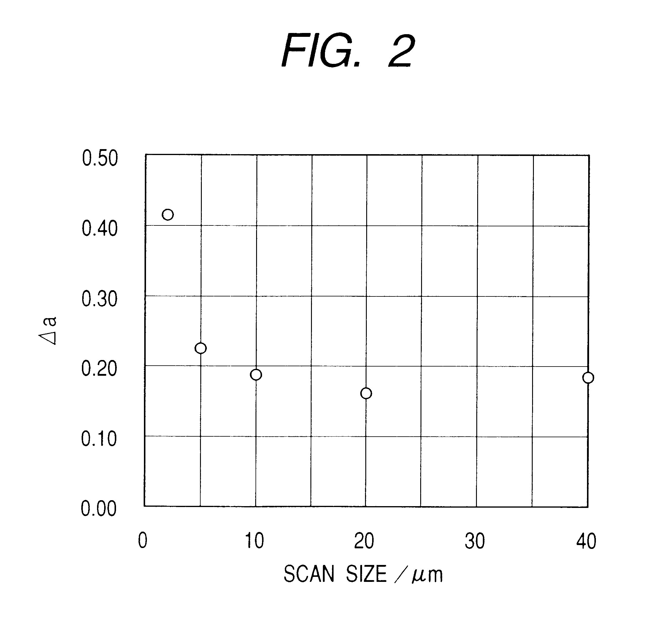
While modifying a forms of a substrate and the parameters of the manufacturing conditions with the above described a-Si photosensitive member film forming apparatus, there were manufactured electrophotographic photosensitive members Nos. 101 through 113 which had different average inclinations .DELTA.a at a measuring level of an AFM and different average inclinations .DELTA.a at a measuring level of a surface roughness meter. Cylindrical substrates made of Al which were used as electrically conductive substrates were subjected to various substrate surface works such as cutting work and dimple work.

Table 1 lists average inclinations .DELTA.a of the photosensitive members Nos. 101 through 113 which were measured within a range of 10 .mu.m.times.10 .mu.m with the AFM, average inclinations .DELTA.a which were measured with the contact type surface roughness meter and results of image evaluation.

In the present invention, the average inclinations .DELTA.a at the measuring level of the sur...

experimental example 2

Then, electrophotographic photosensitive members Nos. 201 through 212 which had different average inclinations .DELTA.a at the measuring level of the AFM and the measuring level of the surface roughness meter and similar photosensitive members Nos. 213 and 214 except that they have no interface were manufactured while modifying the parameters of the manufacturing conditions with the above described a-Si photosensitive member film forming apparatus. Cylindrical substrates made of Al having a purity of 99.9% or higher were used as electrically conductive substrates, which were cut for planished work until microscopic surface roughness Ra was unified not higher than 9 nm.

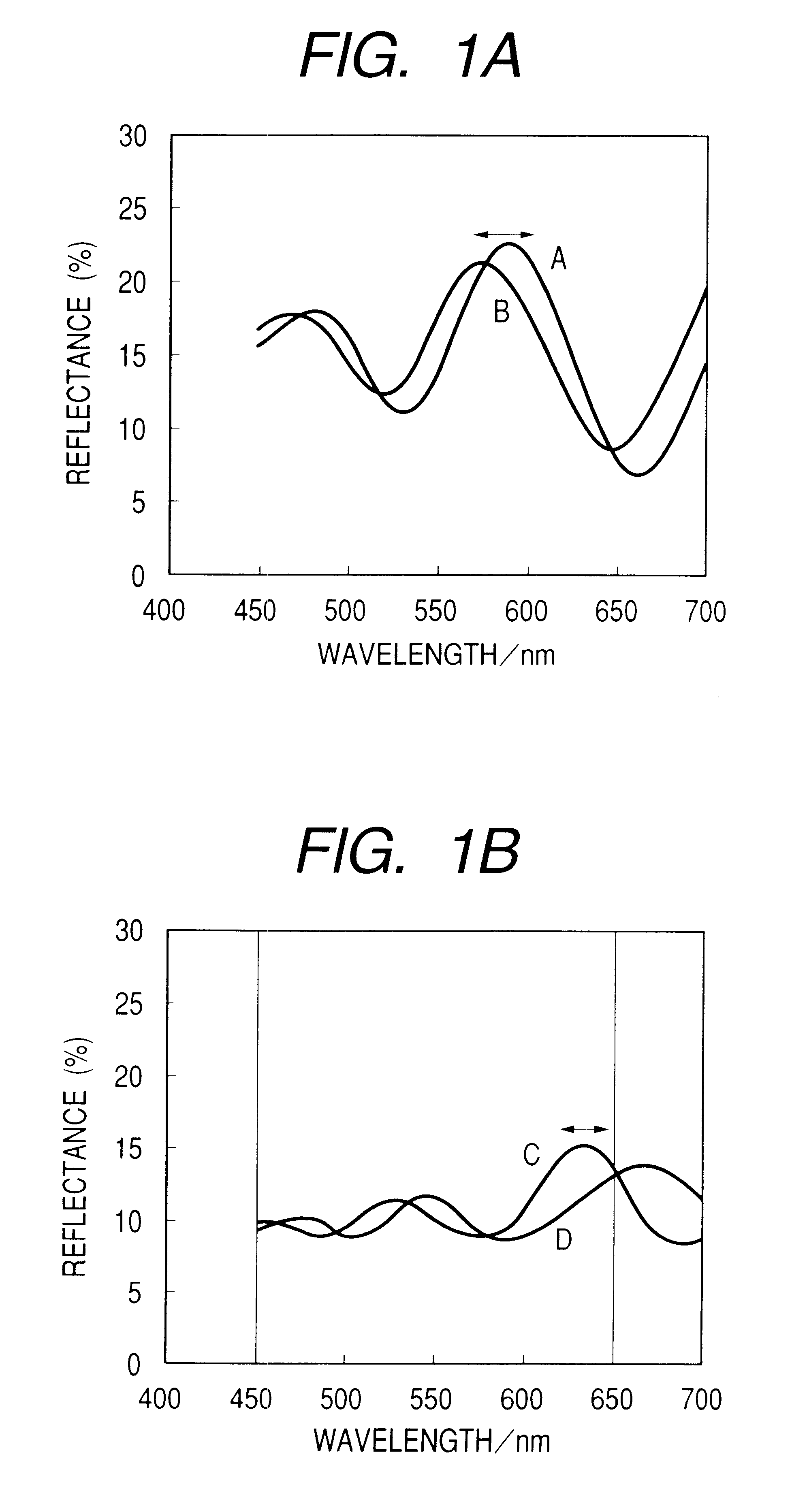
Table 2 lists average inclinations .DELTA.a of the photosensitive members Nos. 201 through 214 which were measured within a range of 10 .mu.m.times.10 .mu.m with the AFM, average inclinations .DELTA.a which were measured with the contact type surface roughness meter, values of reflection on interface according to equat...

experimental example 3

Then, electrophotographic photosensitive members Nos. 301 through 306 were manufactured using electrically conductive substrates which had different microscopic surface roughness Ra as measured in the range of 10 .mu.m.times.10 .mu.m with the AFM. Cylindrical substrates made of Al having a purity not lower than 99.9% were used as the electrically conductive substrates and film forming conditions were adjusted so that average inclinations as measured with the AFM were approximately 0.15 to 0.30.

Table 3 lists microscopic surface roughness Ra of the electrically conductive substrates of the photosensitive members Nos. 301 through 306 and image evaluation results.

As image evaluation, 500,000 sheets were passed for testing durability with a test pattern at a print ratio of 7% using Electrophotographic Apparatus NP6350 manufactured by Cannon and images were evaluated for improper spots. Referred to as improper spots are abnormal partial growth of a film during formation of a photosensitiv...


PUM


Abstract

To provide an amorphous Si photosensitive member and an image forming apparatus which form favorable images by preventing toner adhesion at a cleaning time. A photoconductive layer 102 containing amorphous Si is formed on an electrically conductive substrate 101 so that a surface of a photosensitive member has an average inclination Deltaa within a range of 0.12 to 1.0, more preferably 0.15 to 0.8 within a range of 10 mumx10 mum, and an electrically conductive substrate has surface roughness Ra within the range of 10 mumx10 mum is lower than 9 nm, preferably lower than 6 nm.

Description

1. Field of the InventionThe present invention relates to a photosensitive member and an image forming apparatus, and more specifically a photosensitive member usable for electrophotography which is configured by consecutively laminating a photoconductive layer containing amorphous Si and a surface protective layer, and an image forming apparatus comprising the photosensitive member according to the present invention.2. Related Background ArtAn electrophotographic apparatus comprising an image forming apparatus such as a copier, a facsimile or a printer forms a copied image or the like by uniformly charging an outer circumferential surface of a photosensitive member having a substrate on a surface of which a photoconductive layer is disposed by charging means for roller charging, fur brush charging or magnetic brush charging, and then exposing an image to be copied of an object to be copied to reflected rays, a laser corresponding to a modulated signal or an LED to form an electrost...

Claims


Application Information

Patent Timeline
Patent Type & Authority Patents(United States)
IPC IPC(8): G03G5/147G03G5/082
CPCG03G5/08214G03G5/08221G03G5/08228G03G5/14704G03G5/0825G03G5/147G03G5/08235
Inventor KAWAMURA, KUNIMASAYAMAZAKI, KOJIEHARA, TOSHIYUKIKAWADA, MASAYAKARAKI, TETSUYAOWAKI, HIRONORI
Owner CANON KK
Why Eureka
Try Eureka