Exfoliating method, transferring method of thin film device, and thin film device, thin film integrated circuit device and liquid crystal display device produced by the same

a technology of transferring method and transferring method, which is applied in the direction of semiconductor devices, instruments, optics, etc., can solve the problems of high cost, easy to break, and difficult to produce large transparent substrates from materials

Inactive Publication Date: 2003-11-11
SAMSUNG ELECTRONICS CO LTD
View PDF10 Cites 739 Cited by
  • Summary
  • Abstract
  • Description
  • Claims
  • Application Information

AI Technical Summary

Benefits of technology

In accordance with the present invention, for example, a separation layer having optical absorption characteristics is provided on a substrate having high reliability in device production, and thin film devices such as TFTs and the like are formed on the substrate. Next, although not for limitation, the thin film devices are adhered to a given transfer member, for example, with an adhesive layer, so as to cause an exfoliation phenomenon in the separation layer, which results in a decrease in adhering between the separation layer and the substrate. The substrate is detached from the thin film devices by the force applied to the substrate. A given device with high reliability can be thereby transferred or formed-onto any transfer members.
FIGS. 42(A) to 42(E) are cross-sectional views of another embodiment in which a reinforcing layer is provided to prevent deformation or breakage of a thin film device during exfoliation of a separation layer.

Problems solved by technology

For example, in the production process with high temperature treatment, quartz glass or heat-resisting glass is used, however, they are rare and very expensive materials, and a large transparent substrate can barely be produced from the material.
Further, quartz glass and heat-resisting glass are fragile, easily broken, and heavy.
These are severe disadvantages when a substrate provided with thin film devices such as TFTs is mounted into electronic units.
There is a gap between restriction due to process conditions and preferred characteristics required for products, hence it is significantly difficult to satisfy both the restriction and characteristics.

Method used


Image

  • Exfoliating method, transferring method of thin film device, and thin film device, thin film integrated circuit device and liquid crystal display device produced by the same
  • Exfoliating method, transferring method of thin film device, and thin film device, thin film integrated circuit device and liquid crystal display device produced by the same
  • Exfoliating method, transferring method of thin film device, and thin film device, thin film integrated circuit device and liquid crystal display device produced by the same

Examples


first embodiment

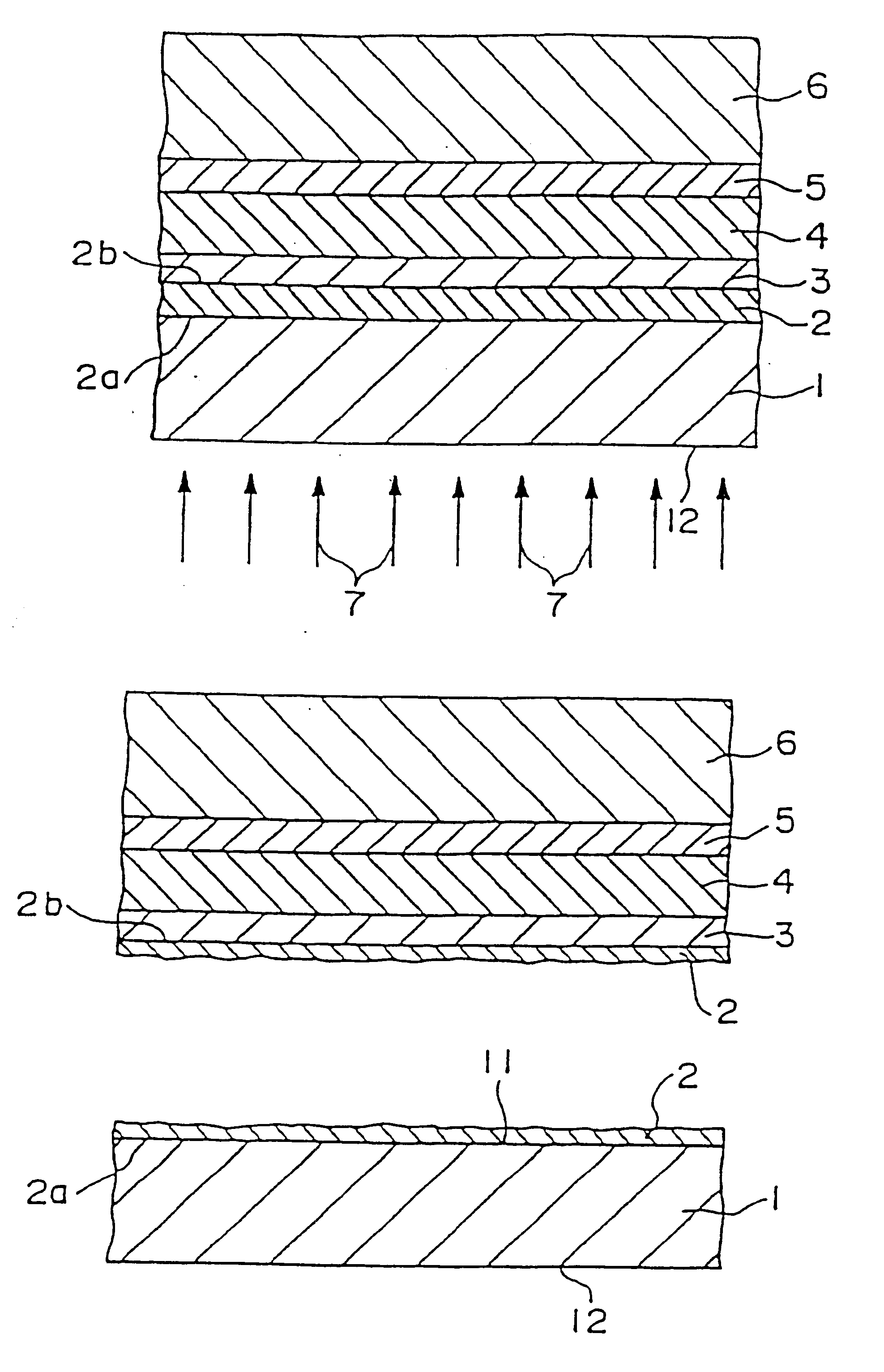
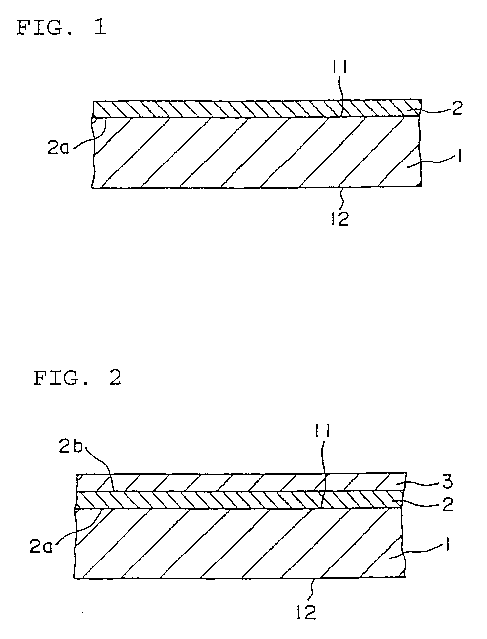
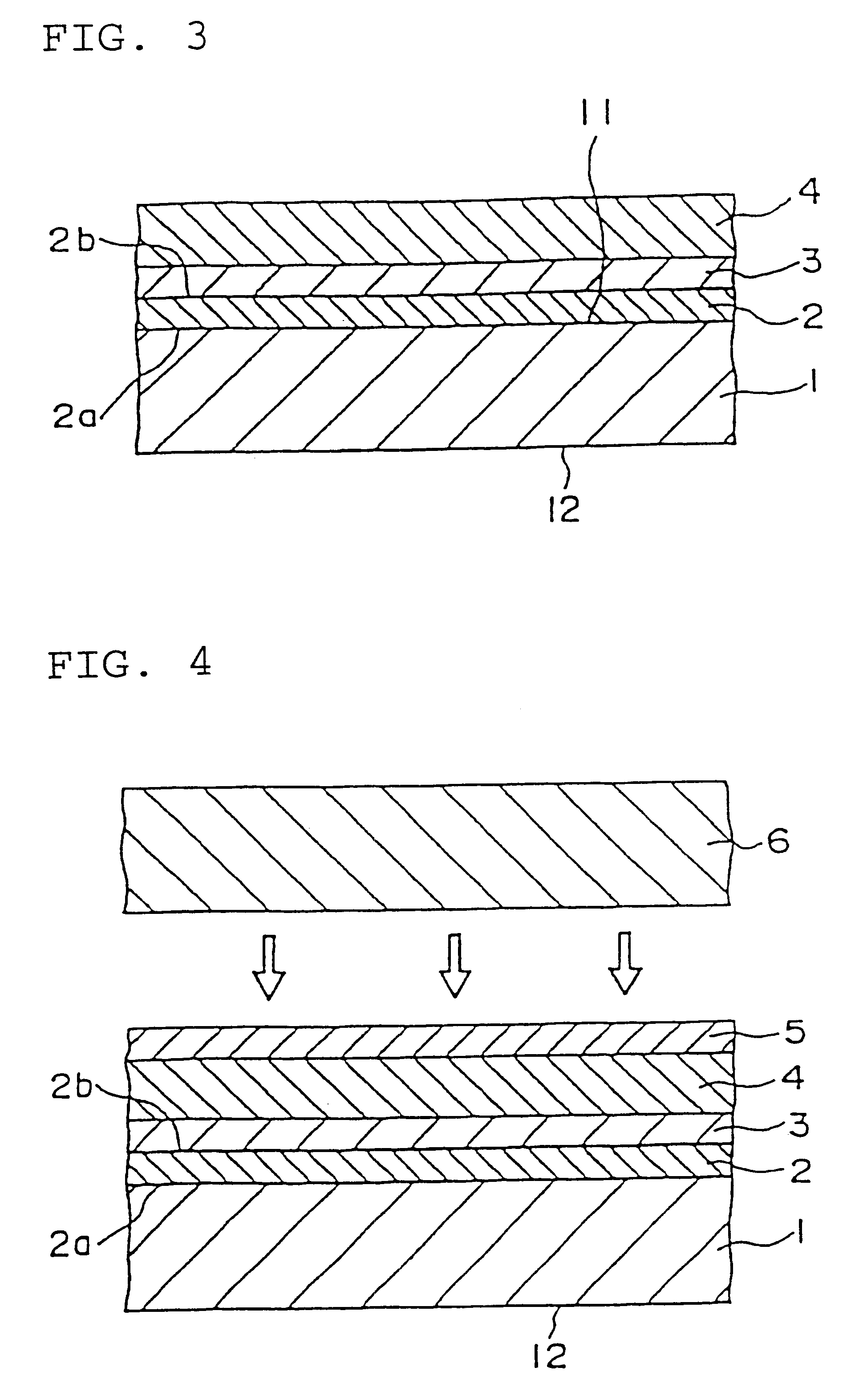
FIGS. 1 to 8 are cross-sectional views of steps in a first embodiment of an exfoliating method in accordance with the present invention. These steps in the exfoliating method (transferring method) in accordance with the present invention will now be described.

[1] As shown in FIG. 1, a separation layer (optical absorption layer) 2 is formed on one side (an inner surface 11 forming exfoliation) of a substrate 1. It is preferable that the substrate 1 has transparency to allow indent light 7 to pass through from the side of the substrate 1. The transmittance of the incident light 7 is preferably 10% or more, and more preferably 50% or more. A significantly low transmittance causes a large loss of the incident light 7, hence a larger amount of light is required for exfoliation of the separation layer 2.

The substrate 1 is preferably composed of a material with high reliability, and particularly composed of a heat-resistant material. When forming a transferred layer 4 and an interlayer 3 a...

example 13

A thin film transistor was transferred as in Example 2, but a transparent AS resin substrate (glass transition point: 70 to 90.degree. C.) as the transfer member was used.

example 14

A thin film transistor was transferred as in Example 3, but a transparent polymethyl methacrylate substrate (glass transition point: 70 to 90.degree. C.) as the transfer member was used.


PUM

PropertyMeasurementUnit
thicknessaaaaaaaaaa
thicknessaaaaaaaaaa
temperatureaaaaaaaaaa

Abstract

A method for transferring a thin film device on a substrate onto a transfer member, includes a step for forming a separation layer on the substrate, a step for forming a transferred layer including the thin film device on the separation layer, a step for adhering the transferred layer including the thin film device to the transfer member with an adhesive layer therebetween, a step for irradiating the separation layer with light so as to form internal and / or interfacial exfoliation of the separation layer, and a step for detaching the substrate from the separation layer.

Description

1. Field of InventionThe present invention relates to a method for exfoliating a detached member, and in particular, a transferring method for exfoliating a transferred layer comprising a thin film such as functional thin film and for transferring it onto a transfer member such as a transparent substrate. Also, the present invention relates to a transferring method of a thin film device, a thin film device, a thin film integrated circuit device, and a liquid crystal display device produced using the same.2. Description of Related ArtProduction of liquid crystal displays using thin film transistors (TFTs), for example, includes a step for forming thin film transistors on a transparent substrate by a CVD process or the like.The thin film transistors are classified into those using amorphous silicon (a-Si) and those using polycrystalline silicon (p-Si), and those using polycrystalline silicon are classified into those formed by a high temperature process and those formed by a low tempe...

Claims


Application Information

Patent Timeline
Patent Type & Authority Patents(United States)
IPC IPC(8): G02F1/13G02F1/1362G02F1/1368H01L21/70H01L27/12H01L21/762H01L21/84H01L21/68H01L21/77
CPCG02F1/13454G02F1/1368H01L21/6835H01L21/76251H01L21/76259H01L27/1214H01L27/1266H01L21/76254G02F2001/13613H01L2221/68363H01L29/78603H01L2221/68359G02F1/13613
Inventor SHIMODA, TATSUYAINOUE, SATOSHIMIYAZAWA, WAKAO
Owner SAMSUNG ELECTRONICS CO LTD
Why Eureka
Try Eureka