Reinforced aluminum copper bonding pad

a bonding pad and aluminum technology, applied in semiconductor devices, semiconductor/solid-state device details, electrical devices, etc., can solve the problems of unprotected bonding pad structure damage, affecting quality, and damage to the bonding pad structur

Inactive Publication Date: 2004-01-13
TAIWAN SEMICON MFG CO LTD
View PDF4 Cites 16 Cited by
  • Summary
  • Abstract
  • Description
  • Claims
  • Application Information

AI Technical Summary

Problems solved by technology

This procedure can damage a bond pad structure, specifically if a raised topography of the bond pad structure is exposed during the wafer thinning procedure.
In addition an unprotected bond pad structure can be damaged in terms of scratches and defects during transporting of the pre-diced semiconductor substrate to an another area of a semiconductor facility in which dicing and wire bonding functions will be performed.
Damaged bond pads can adversely influence the quality of wire bond in terms of increased interface resistance, which in turn deleteriously influence the reliability and yield of a package comprised with individually wire bonded semiconductor chips.

Method used


Image

  • Reinforced aluminum copper bonding pad
  • Reinforced aluminum copper bonding pad
  • Reinforced aluminum copper bonding pad

Examples


Embodiment Construction

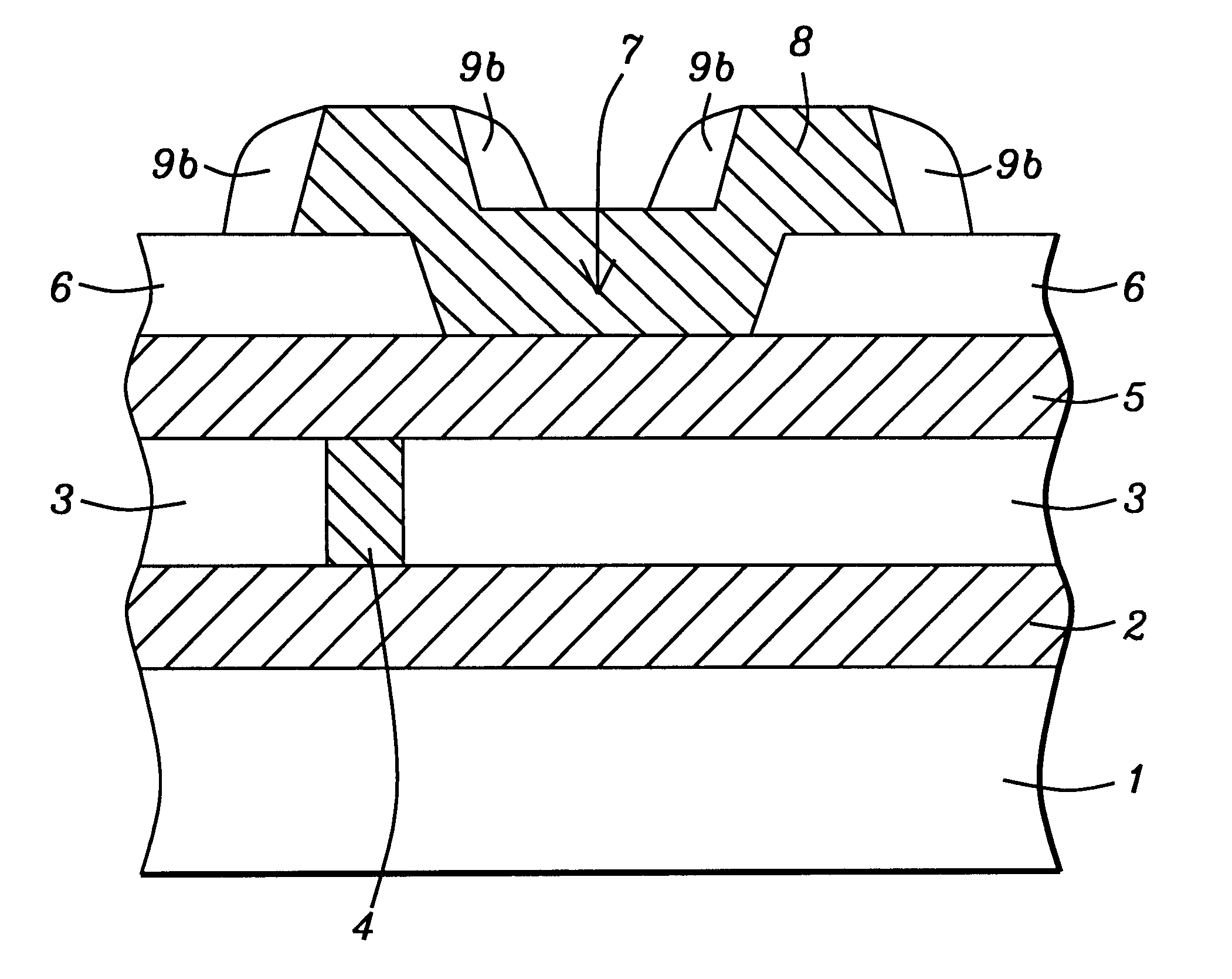
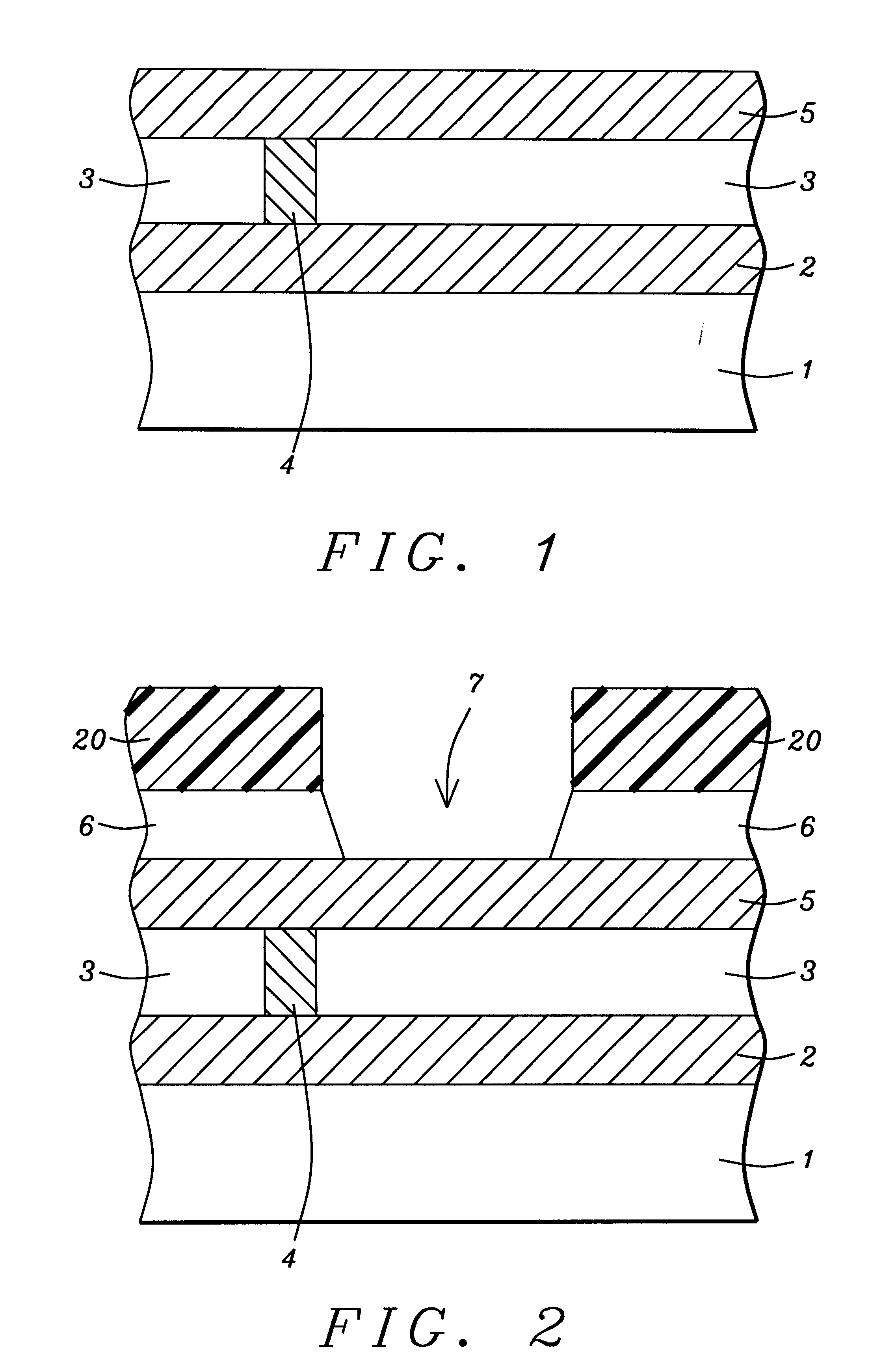
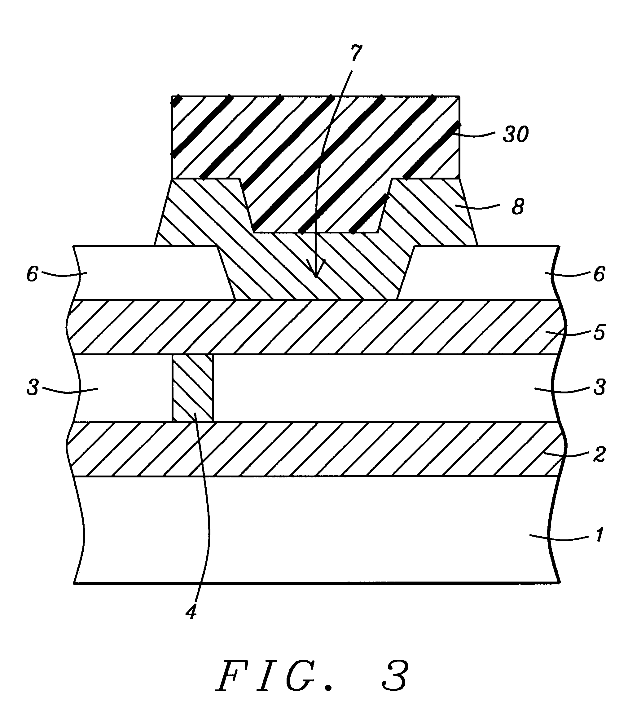
An insulator spacer, reinforced bond pad structure, and a method of forming the bond pad structure featuring insulator sidewall spacers, will now be described in detail. FIG. 1 schematically shows a semiconductor substrate prior to formation of a bond pad structure, featuring interconnect metallization levels, intermetal dielectric (IMD) layers and conductive via structures. Interconnect metal structure 2, located on IMD layer 1, can communicate with lower level interconnect metal structures which in turn contact and communicate with active device regions in a semiconductor substrate, or interconnect metal structure 2 can directly contact the same active device regions of the semiconductor substrate. In this example interconnect metal structure 2, comprised of a conductive layer such as copper, is formed on IMD layer 1, wherein IMD layer 1, in turn is comprised of a dielectric layer such as silicon oxide, phosphosilicate glass (PSG), or boro-phosphosilicate glass (BPSG) with interco...


PUM

PropertyMeasurementUnit
thicknessaaaaaaaaaa
thicknessaaaaaaaaaa
thicknessaaaaaaaaaa

Abstract

A method of forming a bond pad structure reinforced with insulator spacers located on the sides of the bond pad structure has been developed. The method features formation of an aluminum based bond pad structure located overlying and contacting a top portion of a metal interconnect structure exposed in an opening in an intermetal dielectric layer. After deposition of an insulator layer such as silicon nitride or silicon oxide, an anisotropic dry etch procedure is employed to define the insulator spacers on the sides of the bond pad structure. The presence of insulator spacers on the sides of the bond pad structure reduces the risk of bond pad damage which can occur during subsequent pre-wire bonding dicing and transportation procedures.

Description

(1) Field of the InventionThe present invention relates to methods used to fabricate semiconductor devices, and more specifically to a method of forming a bond pad structure employed to accommodate a subsequent wire bond.(2) Description of Prior ArtConnection of a specific semiconductor chip to an external component such as a module or package, can be accomplished via a wire bonding technology which features bonding of a metal wire, such as gold wire, to a specific region of the semiconductor chip with the other end of the wire then connecting to the external component. A critical aspect of the wire bond procedure is the integrity of the semiconductor region, a conductive bond pad structure, to which the wire will be connected to. Bonding pads comprised of conductive materials such as aluminum, have to survive several processes prior to the wire bond procedure. For example the semiconductor wafer comprised with numerous semiconductor chips has to be thinned to approximately to a thi...

Claims


Application Information

Patent Timeline
Patent Type & Authority Patents(United States)
IPC IPC(8): H01L23/485H01L23/48
CPCH01L24/05H01L2924/05042H01L2224/04042H01L2924/01079H01L2924/01029H01L2924/01014H01L2924/01013H01L2224/05073H01L2224/05147H01L2224/05624H01L2224/45144H01L2224/48624H01L24/45H01L2924/00014H01L2924/00
Inventor SU, YEA-ZANHUANG, CHENG-CHUNGHSU, HUAI-JENCHANG, WEN-TSAN
Owner TAIWAN SEMICON MFG CO LTD
Why Eureka
Try Eureka