Manufacturing method of a semiconductor device

a manufacturing method and semiconductor technology, applied in semiconductor devices, semiconductor/solid-state device details, electrical devices, etc., can solve the problems of deterioration in em life em life deterioration, etc., and achieve excellent effect and large aspect ratio

Inactive Publication Date: 2004-01-20
RENESAS ELECTRONICS CORP
View PDF5 Cites 9 Cited by
  • Summary
  • Abstract
  • Description
  • Claims
  • Application Information

AI Technical Summary

Benefits of technology

It is the object of the present invention to provide a formation method of a barrier film which can excellently cope with the hindrance to the EM in connecting an upper and a lower wirings formed of a Cu containing metal in a via hole having a large aspect ratio.

Problems solved by technology

First, in the first conventional structure, voids are generated in the wirings at the bottom part of the via hole which gives rise to a deterioration in the EM life.
Moreover, replenishment of the Cu atoms for compensating the Cu atoms responsible for the formation of the voids is made unavailable, causing a deterioration in the EM life.
This deterioration in the EM life is due to the deterioration of the adhesion at the interface of the barrier film on the side face of the via hole and Cu embedded in the via hole, which is caused by the contamination of the surface of the barrier film during the etch-back of the barrier film.
This leads to an easy generation of the voids, which in turn results in a deterioration in the EM life.
The interface of the barrier film and Cu being the principal diffusion path of Cu atoms by EM, the deterioration in the adhesion of the interface leads to an increase in the diffusion rate of the Cu atoms and to a deterioration in the EM life.

Method used


Image

  • Manufacturing method of a semiconductor device
  • Manufacturing method of a semiconductor device
  • Manufacturing method of a semiconductor device

Examples


Embodiment Construction

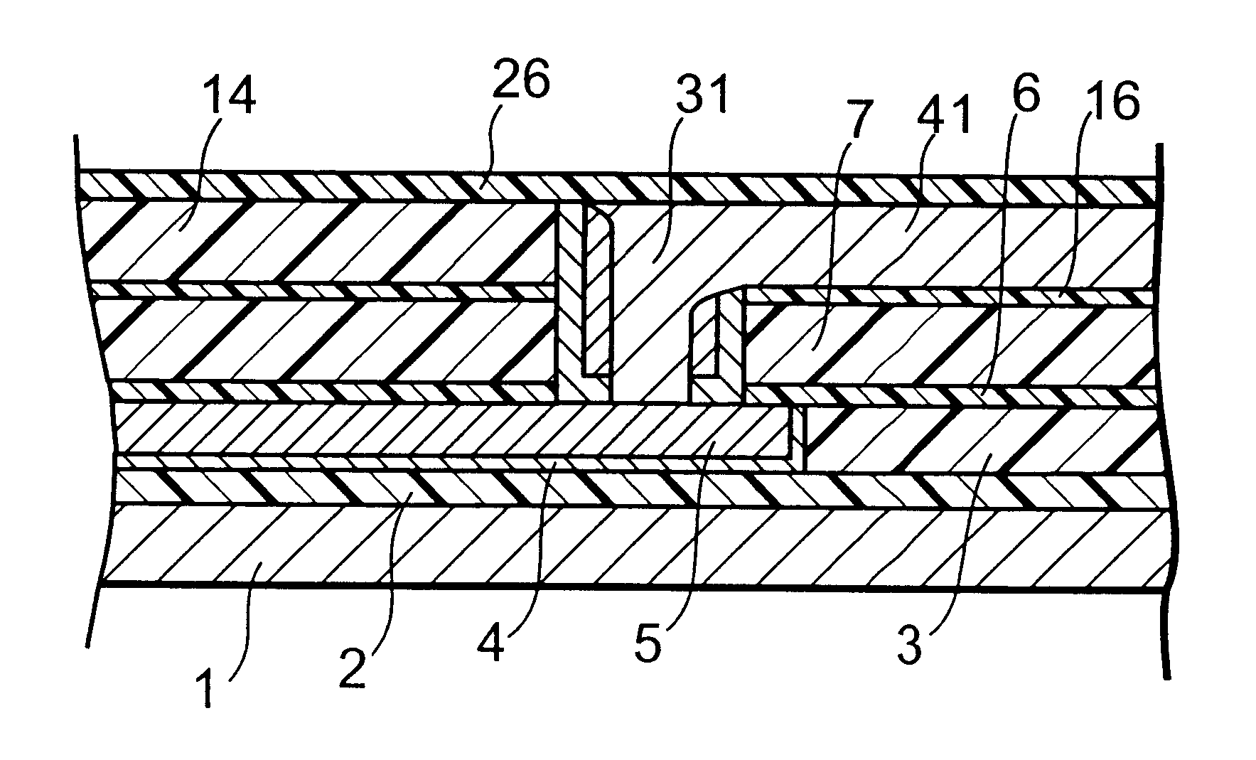
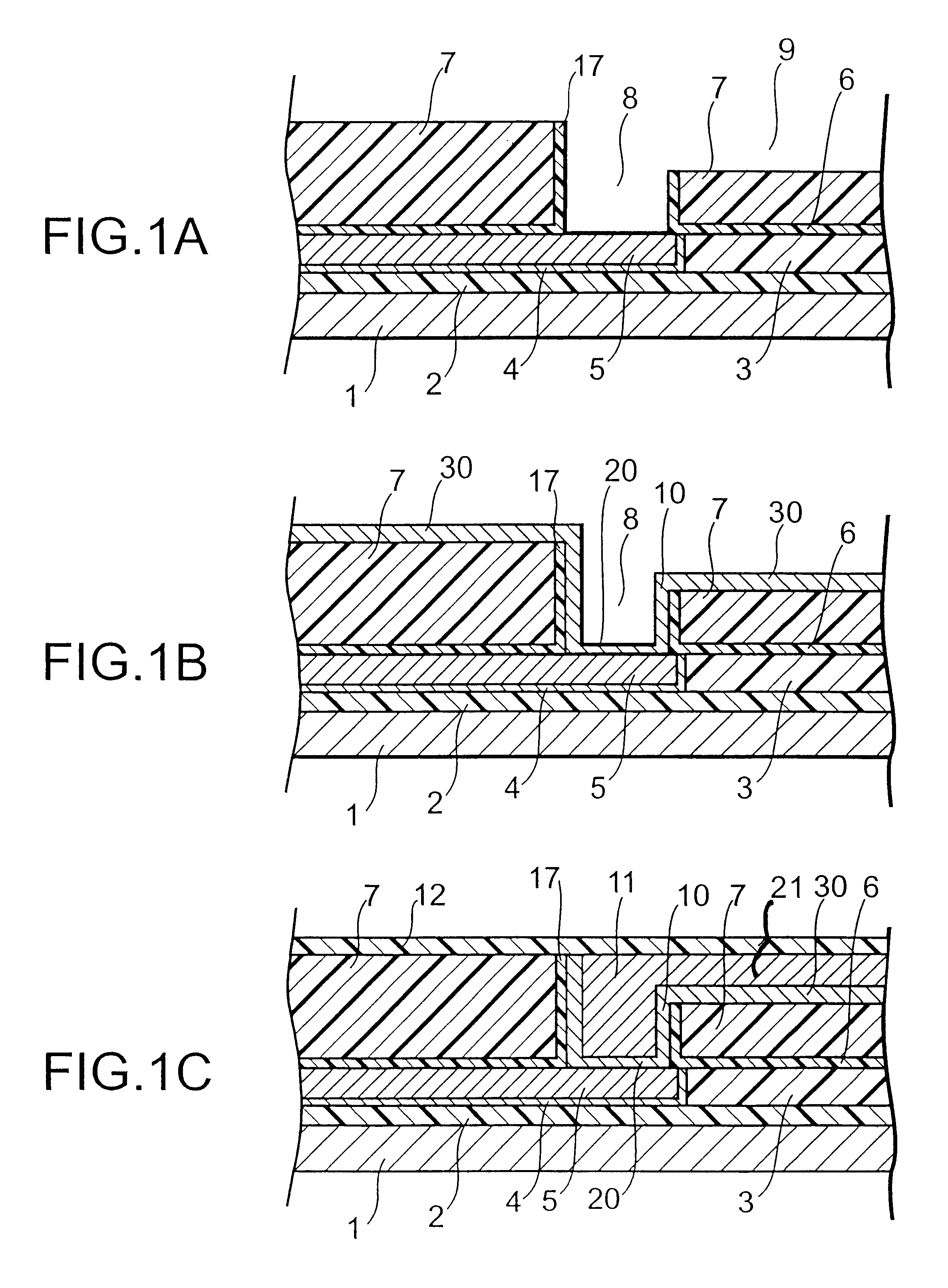
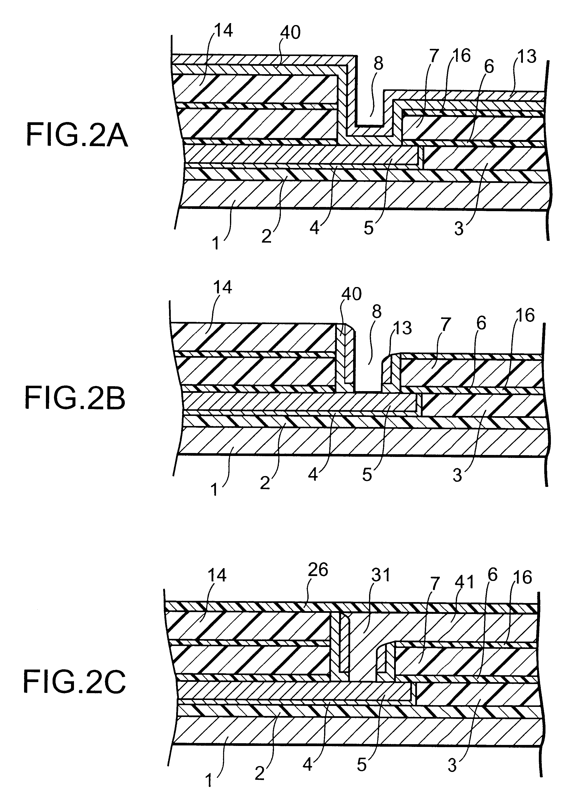
Referring to the sectional views of the manufacturing processes in FIG. 1, a first embodiment of the semiconductor device according to the present invention will be described.

First, a liner insulating film 2 which becomes the base layer of a lower wiring is formed on a semiconductor substrate 1, and a lower wiring 5 is formed on top of it by the damascene method (embedded wiring formation method). The procedure is, first, a first layer insulating film 3 composed of an oxide film is deposited on the liner insulating film 2, and a trench pattern for the lower wiring is formed in the first layer insulating film 3 by photolithography and etching. Then, by sequentially depositing a barrier film of TaN or the like and a lower wiring material composed of Cu or a Cu alloy, and exposing the surface of the first layer insulating film 3 by polishing employing CMP, a barrier film 4 and a lower wiring 5 on are formed on top of it. Then, a nitride film 6 and a second layer insulating film 7 compr...


PUM


Abstract

The manufacturing method of a semiconductor device includes a step of forming a lower wiring on a semiconductor substrate, a step of forming a layer insulating film on the lower wiring, a step of forming an opening that exposes the lower wiring by removing a part of the layer insulating film, a step of forming a barrier film in the opening and a step of forming an upper wiring in the opening, where the lower wiring and the upper wiring are copper including wirings composed of copper or a copper alloy, the barrier film covers the bottom face and the side face of the opening, and the barrier film on the bottom face of the opening is formed so as to have its thickness to be less than twice the diffusion length of the copper atoms in the barrier film.

Description

1. Field of the InventionThe present invention relates to a manufacturing method of a semiconductor device, and more particularly to a formation method of a barrier layer in a semiconductor device having the damascene structure.2. Description of the Prior ArtWhen a metal containing copper is used for both of an upper wiring and a lower wiring, it is necessary to design the manufacturing processes by paying a special attention to electromigration (referred to as EM hereinafter) in the vicinity of a via hole connecting these wirings. What is called EM is a phenomenon in which metal atoms constituting a conductor wiring are transported in the direction of flow of the electrons by the current, and the time from application of stresses of a dc current and temperature to the conductor wiring till the disconnection of the conductor wiring is called EM life.Wiring connection structures in a via hole include the following examples.A first conventional structure is one in which a via plug 111...

Claims


Application Information

Patent Timeline
Patent Type & Authority Patents(United States)
IPC IPC(8): H01L21/02H01L21/4763H01L21/70H01L21/768H01L21/3205H01L23/52
CPCH01L21/76807H01L21/76831H01L21/76843H01L21/76844H01L21/768
Inventor UENO, KAZUYOSHI
Owner RENESAS ELECTRONICS CORP
Why Eureka
Try Eureka