
Method and apparatus for installing a circuit device

a circuit device and installation method technology, applied in the field of methods and equipment, can solve the problems of inconvenient high-speed installation techniques, easy damage to the circuit device package itself during handling and installation, and inability to meet the needs of high-speed installation,

Inactive Publication Date: 2004-01-27
MICRON TECH INC
View PDF17 Cites 6 Cited by
  • Summary
  • Abstract
  • Description
  • Claims
  • Application Information

AI Technical Summary

Benefits of technology

In a favored approach, the technique employs a holder or case designed to enclose the circuit device during transport. The device holder also facilitates placement and alignment of the circuit device for installation. Moreover, the device holder permits ejection of the device for installation without requiring direct contact or handling by the user or service personnel. The technique may be further adapted to facilitate manual installation of a large number of similar devices, such as by vendors, from a tool which stores and ejects a series of similar devices from a stack. In its various embodiments, the technique may be employed with custom-designed component packages, or with packaged circuit devices of conventional design without requiring special adaptation of the external configuration of the packages.
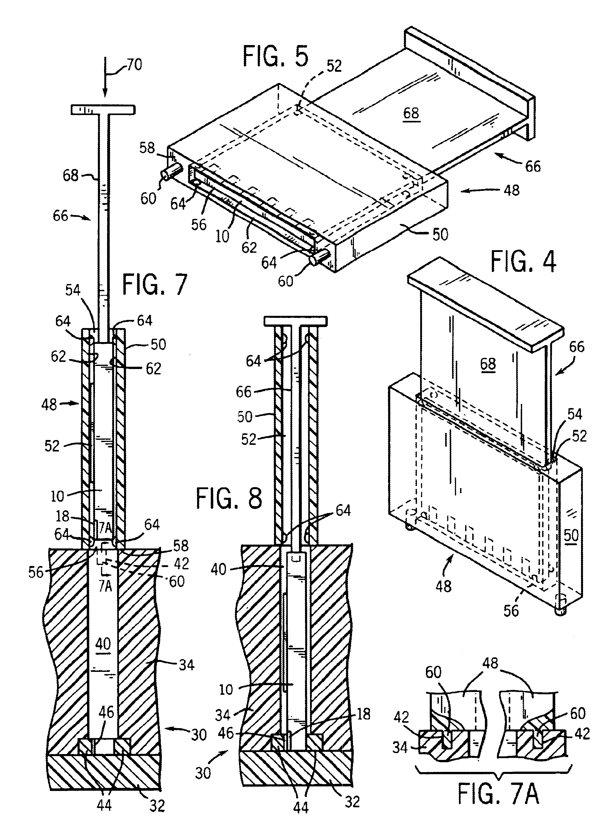
Thus, in accordance with a first aspect of the invention, an apparatus is provided for installing an electronic circuit device on a support. The support includes a plurality of first conductive elements. The device has a plurality of second conductive elements disposed adjacent to at least one edge thereof. The first conductive elements are configured to contact the second conductive elements when the device is installed on the support. The apparatus includes a holder and a manually actuatable ejector. The holder is configured to receive the device and to align the first conductive elements with the second conductive elements. The ejector is configured to extend at least partially into the holder and to urge the device into an installed position wherein the first conductive elements contact respective second conductive elements. The ejector may conveniently include a slot in which the device is aligned. The ejector enters into the slot to press the device from the slot and into engagement on the support upon manual actuation of the ejector. The holder may also conveniently include a plurality of such slots to facilitate transportation, storage and installation of a corresponding number of circuit devices.
In accordance with another aspect of the invention, a tool system is provided for installing a semiconductor device on a receiving support. The device includes a plurality of conductive elements disposed adjacent to an edge thereof. The conductive elements are received by an interface region of the support. The tool system comprises a holder and a manually operated ejector. The holder has side walls forming a cavity for retaining the device. An opening is provided from the cavity for dispensing the device on the support. The ejector is configured at least partially to enter into the cavity and to urge the device through the opening onto the interface region. A second opening may conveniently be provided in the slot for loading or charging the device prior to installation. Features may be provided on the holder which cooperate with registration features on the receiving support to ensure proper alignment of the device with the interface region prior to installation.
The invention also provides a method for installing an electronic circuit device on a support. The circuit device is of the type having a plurality of first conductive elements configured to contact second conductive elements in an interface region of the support. In accordance with the method, the circuit device is positioned in a holder, the holder having a recess for receiving the circuit device. The holder is then positioned on the interface region. The circuit device is manually urged from the recess to electrically couple the first conductive elements to the second conductive elements, thereby installing the circuit device on the interface region of the support. The holder may conveniently guide the circuit device from the recess during its ejection therefrom. During the positioning of the holder on the interface region, registration elements disposed on the holder and the support may be mated to properly align the circuit device over the interface region.

Problems solved by technology

However, for after market or add-on circuits, such high-speed installation techniques are inappropriate.
Such techniques for installing circuit devices suffer from several important drawbacks.
First and perhaps most importantly, the circuit device package itself may be quite fragile and easily damaged during handling and installation.
Similarly, the circuit board and socket on which the package is installed may often be easily damaged when excessive or improperly-directed force is applied to it during installation.
Moreover, increasingly complex add-on circuitry requires a large number of conductive pads or pins extending from the circuit package.
These delicate features of the components stand a much greater risk of damage to either the circuit package or to the support in which the package is installed due, again, to excessive force and misalignment.
In addition, where the circuits are manually handled and installed, serious damage to the circuits can result from static charges inadvertently conveyed to the circuits by the user or service personnel, or from oils present on the installer's hands.
However, such packaging adds to the size and cost of the circuitry, and may not effectively reduce the risk of damage to the circuit on which the add-on package is installed.
Moreover, to the extent that such techniques still require manual handling and installation, risks associated with static charges and oil from handling may be equally unavoidable.

Method used


Image

  • Method and apparatus for installing a circuit device
  • Method and apparatus for installing a circuit device
  • Method and apparatus for installing a circuit device

Examples


Embodiment Construction

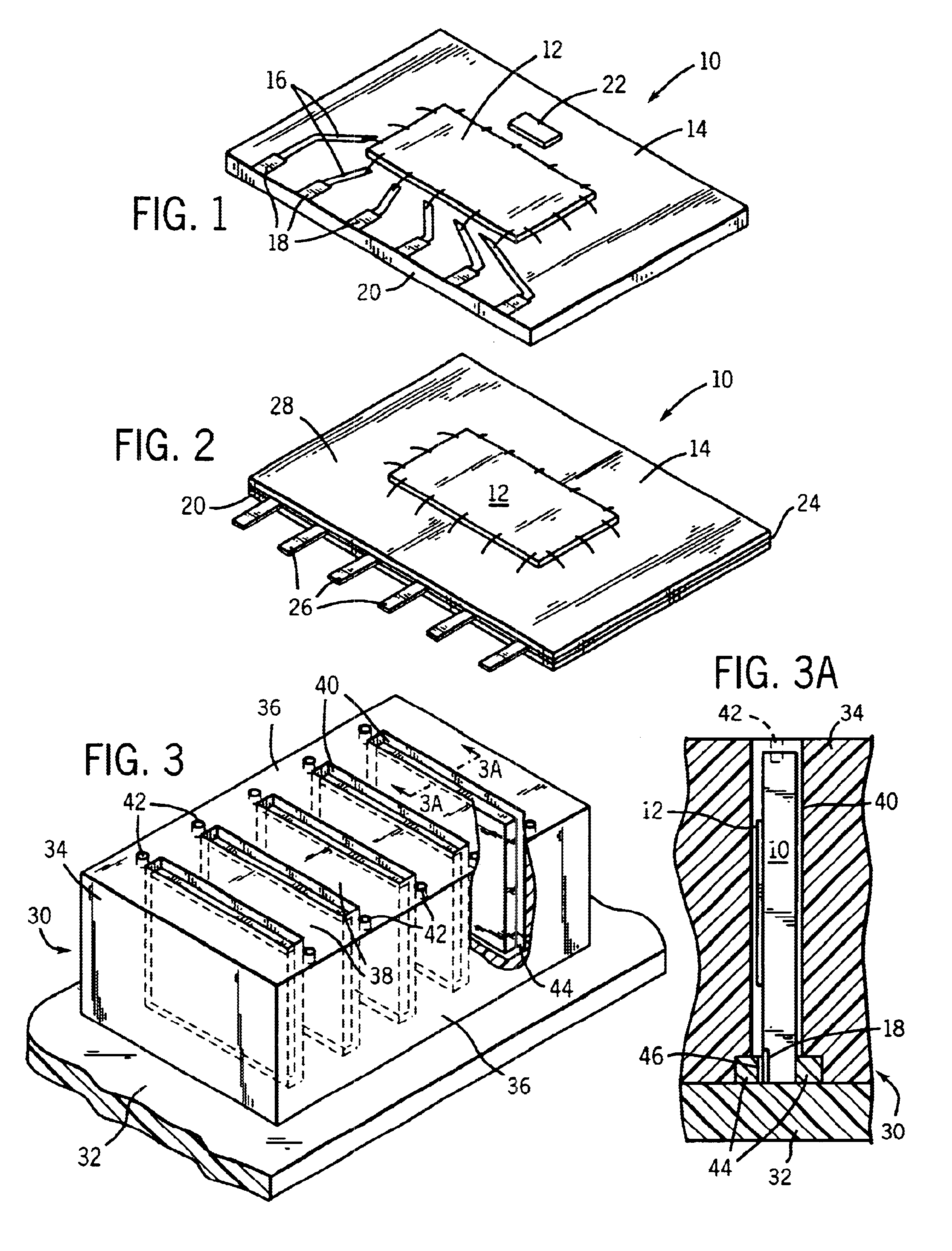
Turning now to the drawings, and referring first to FIG. 1, an electronic circuit device is illustrated and designated generally by the reference numeral 10. Device 10 includes a die 12 in which electronic circuits are formed by conventional processes. Die 12 is supported on a support or substrate 14, and is coupled to electrically conductive traces 16 on the substrate for transmitting power and data signals between circuitry formed in the die and external circuitry. Certain of the conductive traces 16 terminate in conductive pads 18 disposed along one or more edges 20 of substrate 14. In addition to die 12 and conductive traces 16, substrate 14 may include additional circuitry formed on or within a multi-layer structure, or supported on substrate 14. Thus, substrate 14 may include prepackaged surface components 22 designed to electrically interface with circuitry on or in the substrate itself or formed in die 12. Moreover, as will be appreciated by those skilled in the art, device ...


PUM

PropertyMeasurementUnit
Timeaaaaaaaaaa
Forceaaaaaaaaaa
Electrical conductoraaaaaaaaaa

Abstract

A technique is provided for installing circuit components, such as memory devices, in a support, such as a socket. The device to be installed is supported in a holder or shell. The holder is positioned over a support region in the receiving socket. A manual actuator is pressed into the holder to eject the device from the holder and to install the device in the support. The holder may be configured to hold a single device, or multiple devices aligned in slots defined by partitions. A multi-device tray may be provided for indexing devices toward an ejection slot, through which the devices are installed by manual actuation of an ejecting actuator. The technique provides protection for the device prior to and during installation, and facilitates manual installation of such devices without requiring direct hand contact with the device either prior to or during installation.

Description

1. Field of the InventionThe present invention relates to the installation and support of electronic circuits, such as field-installable memory circuits supported in individual packages such as dice, vertical surface mount packages, lead frame packages and so forth. More particularly, the invention relates to a technique for mechanically and electrically installing such circuit devices on a support, such as a socket or connector on a printed circuit board or motherboard.2. Description of the Related ArtA wide variety of packaging techniques have been proposed and are currently in use for supporting and interconnecting electronic circuitry, such as memory devices, add-on peripheral circuits, upgrade circuit components, and so forth. Such devices typically include an electronic circuit or circuits formed in or disposed on a support, such as a semiconductor die. The electronic circuitry on the support is designed to function with external circuitry in the ultimate application, such as ...

Claims


Application Information

Patent Timeline
IPC IPC(8): B25B27/00B25B27/02H05K7/14H05K3/30
CPCB25B27/00H05K7/1415Y10T29/49147Y10T29/53178Y10T29/53191Y10T29/4913Y10T29/49131Y10T29/49222Y10T29/53209Y10T29/53183Y10T29/53257Y10T29/53265Y10T29/49169Y10T29/49133Y10T29/49153Y10T29/49208Y10T29/53174Y10T29/53261H05K3/301
Inventor KINSMAN, LARRYBROOKS, MIKEFARNWORTH, WARREN M.MODEN, WALTERLEE, TERRY
Owner MICRON TECH INC
Learn More