Ink tank and ink jet recording apparatus provided with the same

a technology of ink jet recording apparatus and ink tank, which is applied in the direction of spacing mechanisms, semiconductor devices, printing, etc., can solve the problems of inability to find other information on the inside of the tank, inability to detect residual amount, and inability to use ink

Inactive Publication Date: 2004-02-03
CANON KK
View PDF44 Cites 51 Cited by
  • Summary
  • Abstract
  • Description
  • Claims
  • Application Information

AI Technical Summary

Benefits of technology

In addition, it is another object of the present invention to provide an ink tank that extremely efficiently performing detection of surrounding environmental information and bidirectional exchanges of information with the outside, thereby being capable of detecting detailed information in the ink tank on a real time basis and bidirectionally performing exchanges of information with an ink jet recording apparatus in the outside, and an ink jet recording apparatus provided with the tank.
It is yet another object of the present invention to provide a communication method that is capable of efficiently performing determination and selection of a pair of elements among a plurality of pairs or communication and control between the elements, an ink tank employing the communication method, an ink jet recording apparatus and a communication system.
For example, an electrical contact can be disposed preferably on the part exposed to the outside by embedding the solid semiconductor element in the outer wall. That is, in this way, communication of information between the solid semiconductor element and a recording apparatus main body, supply of energy for activating the solid semiconductor element or the like can be performed via a contact provided in a part supporting the ink tank. In addition, the information communicating means can be disposed preferably in the part exposed to the outside, which can acquire an advantage of being capable of efficiently communicating a signal to the outside because it is exposed to the outside. In this case, the solid semiconductor element is disposed such that it can be seen from the outside, whereby a user can directly confirm information from the information communicating means with the information communicating means as means for communicating information to the outside by a visually recognizable method such as emitting light.
In this way, since a function of acquiring surrounding environmental information to communicate it to the outside is incorporated in a semiconductor element of a solid shape, information can be acquired and communicated three-dimensionally. Thus, a direction of communicating information is not limited compared with the case in which a semiconductor element of a flat shape is used. Therefore, surrounding environmental information can be efficiently acquired and communicated to the outside.
In addition, when a plurality of solid semiconductor elements are disposed in a predetermined container to communicate with a plurality of groups of elements with two or more solid semiconductor elements among the plurality of solid semiconductor elements in the predetermined container forming one group, communication is performed with a different communication condition for each of the element groups. As a result, it becomes possible to efficiently performing determination and selection of a pair of elements among the plurality of pairs and communication and control between the elements. Alternatively, each of the plurality of solid semiconductor elements provided in the predetermined container has information for distinction or a memory, and communication is performed by recognizing the information for distinction or distinguishing the information by the memory. Thus, it also becomes possible to efficiently performing determination and selection of a pair of elements among the plurality of pairs and communication and control between the elements.
In addition, more than two solid semiconductor elements of this kind are disposed in an ink tank, and environmental information of the surrounding of the semiconductor solid elements is detected by mutually communicating between the two or more solid elements, and the environmental information is communicated to and displayed in the outside. Thus, it is possible to communicate information on ink contained in the ink tank, a pressure in the tank or the like to, for example, an ink jet recording apparatus in the outside on a real time basis. This is advantageous in controlling, for example, an amount of negative pressure that changes every moment in accordance with ink consumption to stabilize discharge of ink jet.

Problems solved by technology

In addition, since the ink residual amount is detected by a conduction state between the electrodes, there is a restriction on ink to be used as indicated by the fact that a metal ion cannot be used as an ink component, or the like.
In addition, only the ink residual amount can be detected and the other information on the inside of the tank cannot be found from the outside in the above-mentioned configurations.
In addition, in order to make this element effectively applicable to the ink tank, there were problems that should be cleared.
One of the problems is supply of electricity for activating the element contained in the tank.
As a result, since manufacturing costs of the tank increases and a tank cartridge becomes expensive, a user has to activate the element from the outside without contacting it or has to activate the element by directly contacting it.
In addition, it is not conventionally known that a user communicates information between two elements disposed in remote places without contacting them or communicates with and controls a configuration that is provided with, for example, a plurality of pairs consisting of two elements.
According to this embodiment, since the element has means for directly communicating information, it is sufficient to supply electricity only, and excess electric wiring is unnecessary.
In addition, since the element has the energy converting means, it becomes unnecessary to dispose means for storing electromotive force for activating the element (a power source in this example).

Method used


Image

  • Ink tank and ink jet recording apparatus provided with the same
  • Ink tank and ink jet recording apparatus provided with the same
  • Ink tank and ink jet recording apparatus provided with the same

Examples


seventh embodiment

(Seventh Embodiment)

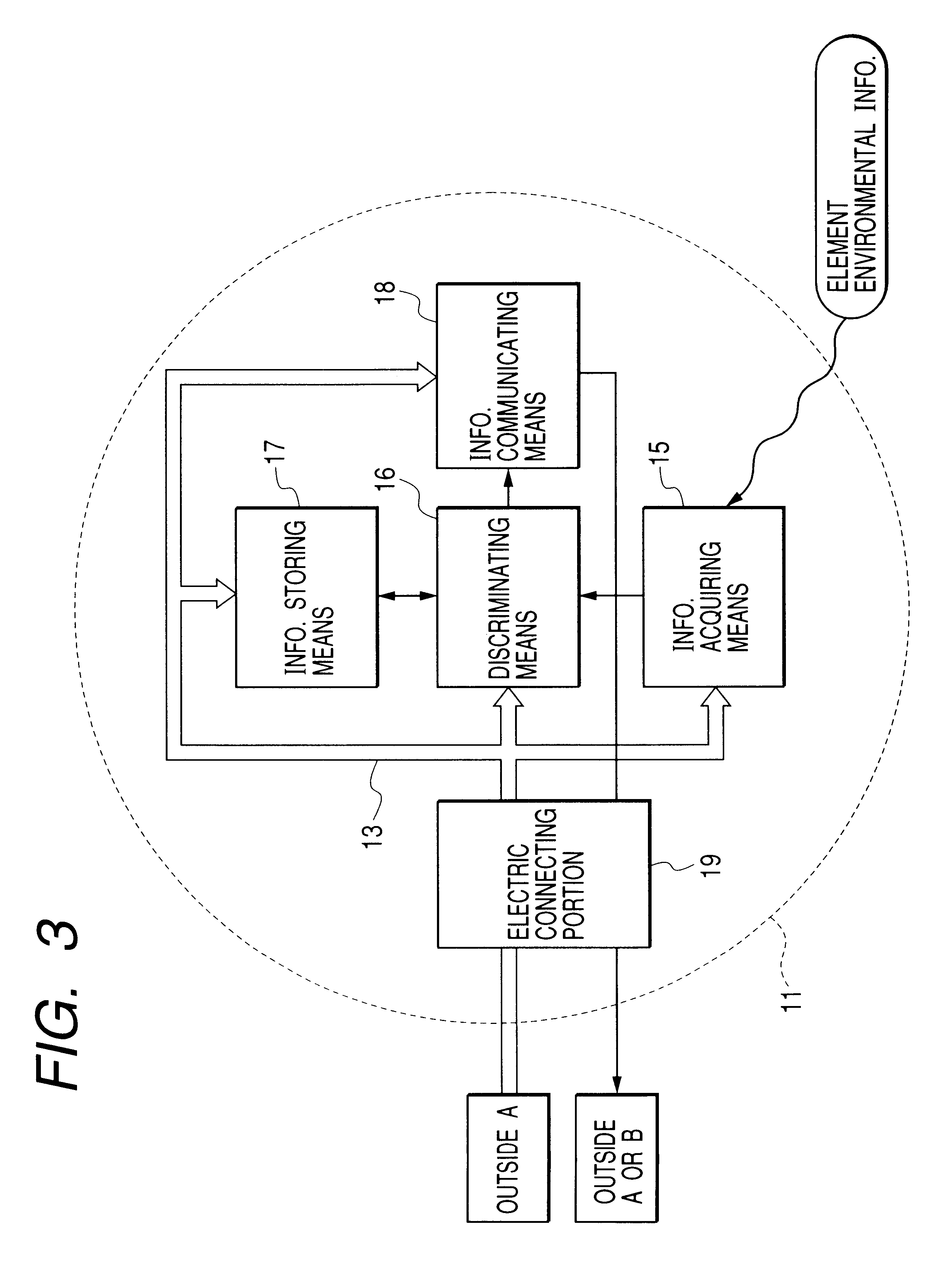
FIG. 23 is block diagram illustrating an internal configuration and exchanges of information with the outside of a solid semiconductor element according to a seventh embodiment of the present invention. A solid semiconductor element 31 of a form shown in this figure is provided with energy converting means 34 for converting electromotive force 32 supplied in a non-contact state from the outside A toward the element 31 into electricity 33 and buoyance force generating means 35 for generating buoyance force using the electricity acquired by the energy converting means 34, and is disposed in ink in an ink tank.

In such a form, when the electromotive force 32 is given from the outside A toward the element 31, the energy converting means 34 converts the electromotive force 32 into the electricity 33, and the buoyance force generating means generates buoyance force using the electricity 33 to float the element 31 on the liquid level of the ink. This buoyance force not o...

eighth embodiment

(Eighth Embodiment)

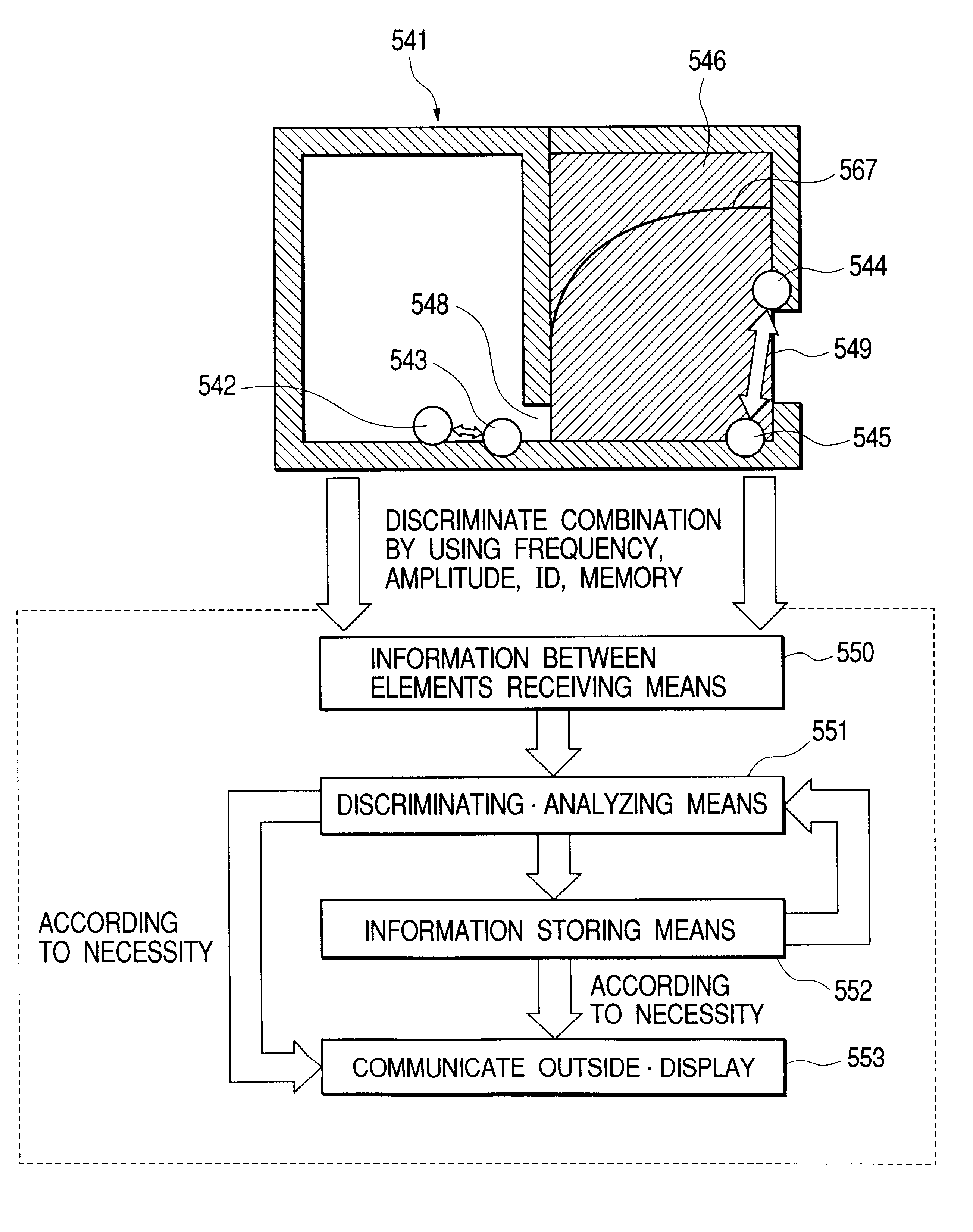
FIGS. 26A to 26C are conceptual drawings illustrating a method of using two or more, that is, a plurality of solid semiconductor elements, which is an eighth embodiment of the present invention.

This embodiment has a configuration in which a function of communicating information to the other elements is given to the solid semiconductor elements of the first and the sixth embodiments, a plurality of which are disposed in an object.

In an example of FIG. 26A, a plurality of solid semiconductor elements of the first embodiment are disposed in an object. When electromotive force is supplied form the outside A or B to each element, each element acquires surrounding environmental information, respectively. Then, information acquired by an element 41 is communicated to an element 42, information a and b acquired by the element 41 and the element 42, and subsequent information is sequentially communicated to the next element. A last element 43 communicates all information a...


PUM


Abstract

An ink tank is provided which can efficiently perform detection of information in an ink tank such as an ink residual amount in the ink tank with a simple configuration in which it is unnecessary to set wiring or the like. A solid semiconductor element, which is provided with an acquiring unit for acquiring environmental information of the outside, an information storing unit, a discriminating unit for comparing acquired information and stored information to make a determination, and an information communicating unit for displaying the acquired information or communicating the acquired information to the outside, is embedded in an outer wall of an ink tank such that the solid semiconductor element is exposed to an internal side and an external side of the ink tank from the outer wall. The solid semiconductor element can perform supply of its operation energy or exchanges of signals in a non-contact state or by connecting with a terminal provided in a supporting portion or the like of the ink tank directly, thus, it is unnecessary to set wiring. In this case, the information acquiring means can be preferably disposed in the part of the solid semiconductor element exposed to the inside of the ink tank.

Description

1. Field of the InventionThe present invention relates to an ink tank provided with a semiconductor element having functions of detecting environmental information of the surroundings to communicate the information to the outside and display the same, or having functions of detecting information inside an ink tank (e.g., an ink residual amount) using a semiconductor element to communicate the information to the outside and display the same.In addition, the present invention relates to an ink jet recording apparatus such as a facsimile machine, a printer and a copying machine to which the ink tank is detachably mountable.2. Related Background ArtConventionally, in an ink jet recording apparatus for printing an image on a sheet with dot patterns by moving a carriage, which is provided with a recording head, in a printing direction while jetting ink from a plurality of jet nozzles provided in the recording head, an ink tank containing ink for recording is provided and the ink in the in...

Claims


Application Information

Patent Timeline
Patent Type & Authority Patents(United States)
IPC IPC(8): B41J19/20B41J2/195B41J2/17B41J2/175B41J29/393B41J2/01H01L25/00
CPCB41J2/17513B41J2/17546B41J2/17556B41J2/17566B41J2/17596B41J2/195B41J19/202B41J29/393B41J2002/17583B41J2202/17B41J2/00
Inventor MOCHIZUKI, MUGASAITOISHINAGA, HIROYUKIIMANAKA, YOSHIYUKIKUBOTA, MASAHIKOINOUE, RYOJIYAMAGUCHI, TAKAAKI
Owner CANON KK
Why Eureka
Try Eureka