Image sensor

a technology of image sensor and metal oxide semiconductor, which is applied in the field of metal oxide semiconductor image sensor, can solve the problems of shrinking the dynamic range of output signal

Inactive Publication Date: 2004-02-10
RENESAS ELECTRONICS CORP
View PDF4 Cites 219 Cited by
  • Summary
  • Abstract
  • Description
  • Claims
  • Application Information

AI Technical Summary

Problems solved by technology

Therefore, such a problem occurs that a dynamic range for an output signal shrinks.
Moreover, since the transistor 1 is provided with the step-up level of VDD+Vt, a gate oxide film, for example, must be increased in thickness, to assure a high breakdown voltage, which leads to another problem.
Therefore, such a problem occurs that a dynamic range for output signals shrinks.
Also, since the transistors 1 and 6 are provided, at their gate, with the step-up level VDD+Vt, a gate oxide film, for example, must be increased in thickn

Method used


Image

  • Image sensor
  • Image sensor
  • Image sensor

Examples


second embodiment

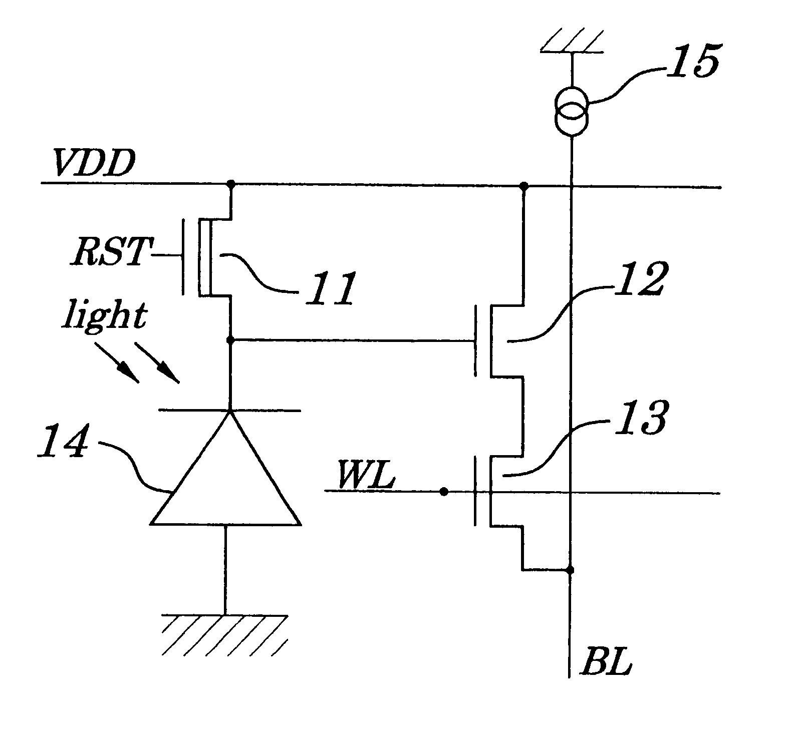
FIG. 3 shows a configuration of a unitary pixel circuit in an image sensor according to a second embodiment of the present invention, in which the circuit is made of n-channel transistors.

The pixel circuit shown in this example roughly comprises a resetting transistor 11A, an amplifying transistor 12A, a bit-line output transistor 13, a photo-diode 14, and a current source 15.

In this configuration, the transistors 12A and 13 are of an enhancement type, of which the transistor 12A is supposed to be of a high-breakdown voltage type. The transistor 11A is a depletion-type one having a high-breakdown voltage.

When the Reset signal RST went high, the transistor 11A supplies a step-up supply voltage VBOOT to the photo-diode 14, thereby resetting it to the photo-electric conversion initiation state. The transistor 12A forms a source follower together with a current source 15, thus amplifying a photo-electric conversion voltage of the photo-diode 14. When a word-line readout control signal W...

third embodiment

FIG. 4 shows a configuration of a unitary pixel circuit in an image sensor according to a third embodiment of the present invention, in which that circuit is made of n-channel transistors.

This exemplary pixel circuit roughly comprises a resetting transistor 11, an amplifying transistor 12, a bit-line output transistor 13, a photo-diode 14, a current source 15, and a transfer gate transistor 16. In this configuration, the transistors 12 and 13 are of an enhancement type, while the transistor 11 and 16 are of a depletion type.

In this example, the transistors 11, 12, and 13 as well as the photo-diode 14 and the current source 15 are the same as those of the first embodiment shown in FIG. 1, with a large difference that the transistor 16 constituting the transfer gate is provided in series with the photo-diode 14. Although the transistor 16 usually disconnects the photo-diode 14 from an interconnection between a source of the transistor 11 and a gate of the transistor 12, when a gate si...

fourth embodiment

FIG. 6 shows a configuration of a unitary pixel circuit in an image sensor according to a fourth embodiment of the present invention, in which the circuit is made of n-channel transistors.

The pixel circuit in this example roughly comprises a resetting transistor 11A, an amplifying transistor 12A, a bit-line output transistor 13, a photo-diode 14, a current source 15, and a transfer gate transistor 16A. Of these, the transistors 12A and 13 are of an enhancement type, while the transistor 12A is of a high-breakdown voltage type. The transistors 11A and 16A are depletion-type transistors having a high breakdown voltage.

When the Reset signal RST went high, the transistor 11A supplies a step-up supply voltage VBOOT to the photo-diode 14, to reset it to a photo-electric conversion initiation state. The transistor 12A forms a source follower together with the current source 15, to amplify a photo-electric conversion voltage of the photo-diode 14. When a word-line readout control signal WL ...


PUM


Abstract

According to an image sensor disclosed, a pixel circuit includes a photo-diode 14 for generating a photo-electric conversion voltage which corresponds to an input optical level, a transistor 11 which is activated in response to a Reset signal RST, to initialize the photo-diode 14 from a power supply VDD, a transistor 12 which, when connected between the power supply VDD and a bit line BL, amplifies a photo-electric conversion voltage and outputs it onto the bit line BL, and a transistor 13 which is activated by a word-line readout control signal WL, to interconnect the transistor 12 and the bit line BL, in which the transistor 11 is of a depletion type.

Description

1. Field of the InventionThe present invention relates to an MOS (Metal Oxide Semiconductor) type image sensor and, more particularly, to such an image sensor that uses depletion-type transistors as a group of transistors for initializing a pixel light-receiving unit.2. Description of the Related ArtAn image sensor is used in a TV camera etc. for converting into an electric signal the optical image information taken in from outside, by such a configuration that a large number of pixels are arranged in a matrix-shaped plane. An MOS-type image sensor has a photo-diode or photo-transistor as its photo-electric conversion unit and also does it comprise a pixel circuit as its peripheral circuit configured with MOS-type FETs (Field Effect Transistors), thus featuring reduced power dissipation, cost, etc. as compared to a traditional popular CCD (Charge Coupled Device).In a conventional MOS-type image sensor, it has been quite common to use enhancement-type transistors easy to manufacture ...

Claims


Application Information

Patent Timeline
IPC IPC(8): H04N3/15H01L27/146H04N5/335H04N5/355H04N5/359H04N5/361H04N5/369H04N5/374H04N5/3745
CPCH04N5/3594H04N5/374H04N25/623H04N25/76
Inventor MURAMATSU, YOSHINORIKUROSAWA, SUSUMUNAKASHIBA, YASUTAKANAGATA, TSUYOSHI
Owner RENESAS ELECTRONICS CORP
Why Eureka
Try Eureka