

Electrically erasable, programmable, non-volatile memory device compatible with a CMOS/SOI production process
a non-volatile memory, programmable technology, applied in the direction of semiconductor devices, electrical apparatus, transistors, etc., can solve the problems of limited type of memory cells and tunnel oxide reliability problems
- Summary
- Abstract
- Description
- Claims
- Application Information
AI Technical Summary
Benefits of technology
Problems solved by technology
Method used
Image

Examples
Embodiment Construction
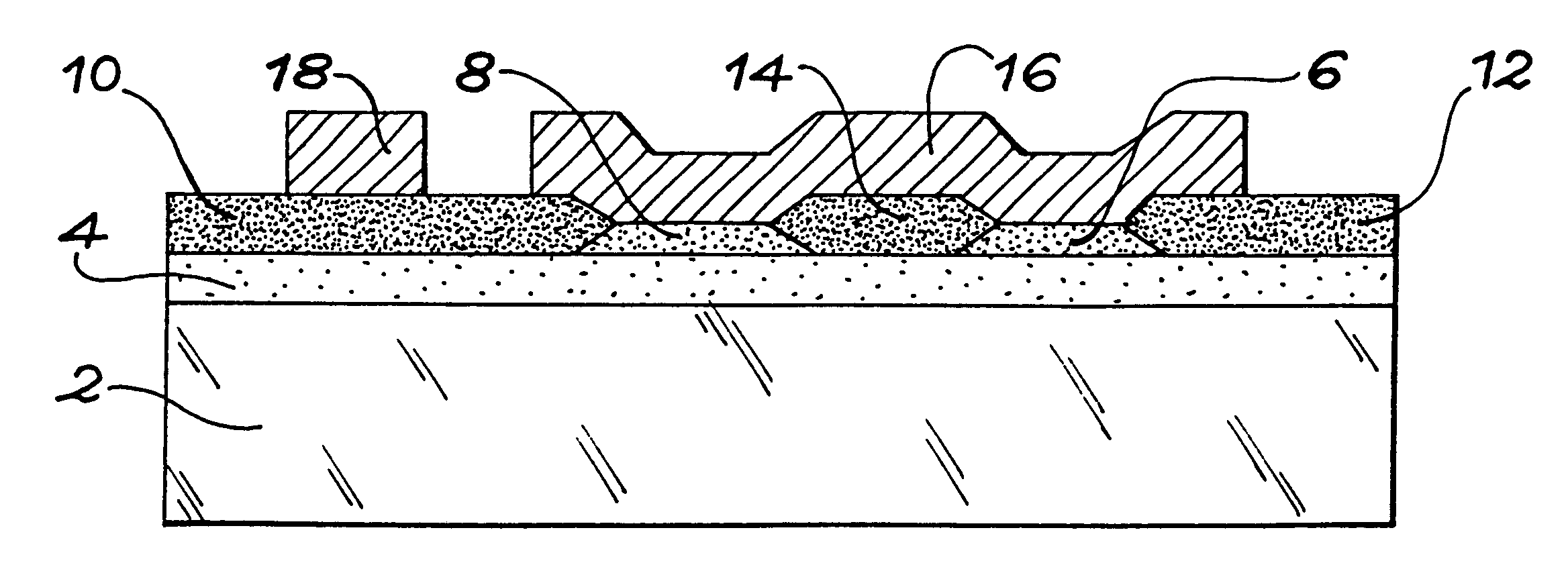
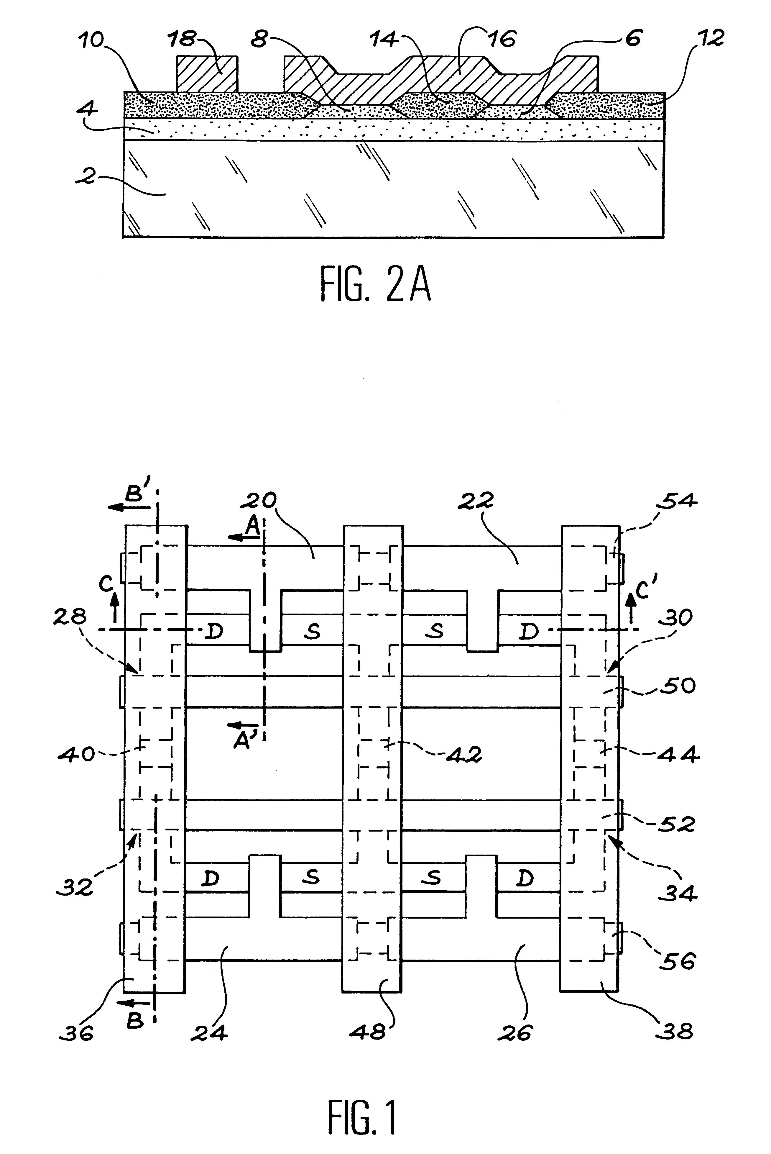
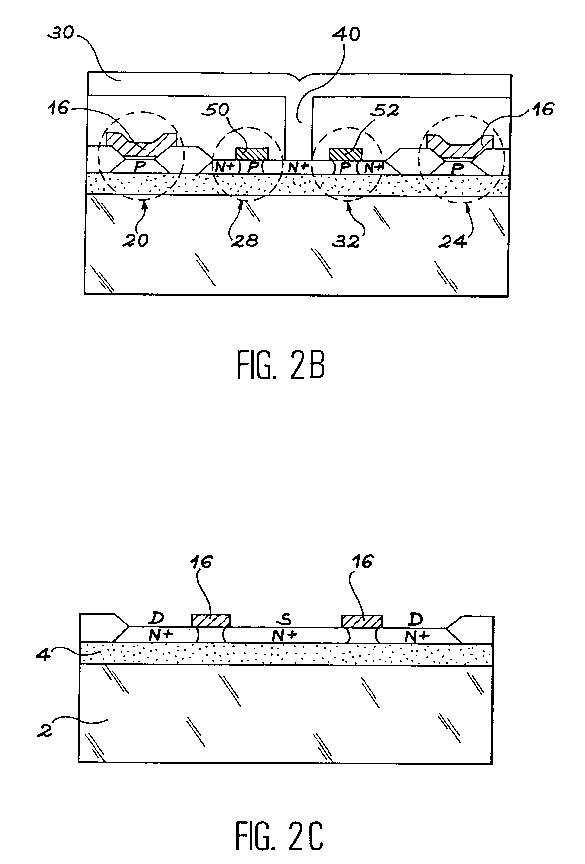
The present invention relates to a non-volatile memory cell, e.g. of the electrically bit by bit programmable and erasable EEPROM type and having the special feature of being conventionally implementable in a CMOS / SOI process. In addition, the memory cell surface area is preferably small.
More specifically, the invention relates to an electrically erasable, non-volatile memory device, having a memory cell of the floating gate type, defined by a source zone, a drain zone, a channel zone and a control gate zone, the latter being separated from the channel zone by an insulation zone, said five zones being implemented in a semiconductor film formed on an insulating layer, said memory cell being laterally insulated by one or more insulation zones in contact with the insulating layer.
The invention also relates to an electrically erasable, non-volatile memory device having, in a semiconductor film separated by an insulating layer from a substrate, at least one memory cell laterally insulate...
PUM
 Abstract
Description
Claims
Application Information