
Single wafer megasonic cleaner method, system, and apparatus

a single-wallet, mega-sonic technology, applied in the direction of cleaning using tools, cleaning using liquids, chemistry apparatus and processes, etc., can solve the problems of reducing the reliability and yield of the fabrication facility, many substrates are delicate, and can no longer be cleaned with brushes

Inactive Publication Date: 2004-05-04
KUYEL BIROL
View PDF5 Cites 45 Cited by
  • Summary
  • Abstract
  • Description
  • Claims
  • Application Information

AI Technical Summary

Benefits of technology

"The present invention relates to an improved method and apparatus for cleaning microelectronic workpieces by removing submicron-sized contaminants from the surface of the workpiece using megasonic energy. The invention addresses the challenges of effectively cleaning contaminants from semiconductor devices as they become smaller and more difficult to remove. Prior art methods have used brushes and high-pressure water jets which have limitations including causing damage to metal patterns on wafers and requiring large quantities of cleaning fluid. The invention aims to overcome these shortcomings by using a megasonic nozzle system that can apply energy to the entire surface of the workpiece without causing energy density gradients or reattachment of contaminants. The invention also includes a drying process to effectively remove cleaning fluid from the workpiece to prevent contamination and reattachment of particles."

Problems solved by technology

Even extremely small foreign particles may cause fatal defects during the fabricating process, thereby decreasing the reliability and yield of the fabrication facility.
These submicron-sized particles are difficult to displace because of strong adhesion forces between the particles and the substrate, such as caused by Van der Waals forces, capillary forces, chemical bonding, and / or electrostatic forces.
However, with the increased level of miniaturization, many substrates are delicate and can no longer be cleaned with brushes.
Brushes are abrasive, and the metalization on wafers and masks cannot tolerate such abrasive cleaning processes.
Often, however, the high pressure within the water column causes damage due to the large forces they exert, particularly to metal patterns on the wafers.
Additionally, high-pressure water jets typically require large quantities of deionized water, which may not be economical for a manufacturing environment.
Ultrasonic cleaning causes cavitation effects, and therefore results in micro explosions that are undesirable for today's microchip manufacturing.
However, removing cleaned articles from a tank is problematic because particles frequently reattach to the surface as the article is being removed.
Another problem is that the tank itself is an acoustical cavity, with standing waves, peaks, and valleys.
Further, the energy coupled to the tank is affected by the loading of the tank.
Additionally, energy density is limited due to the fact that all energy has to distribute to the full volume of the tank.
An additional drawback to cleaning semiconductor parts in a tank is the large quantities of cleaning fluids required.
These chemicals are expensive and generally hazardous to the environment.
However, during cleaning, the system in the '647 patent rotates the substrate at high RPMs.
Use of high-RPM cleaning has a number of disadvantages including inherent non-uniformity of the energy delivered (particularly at low radial lengths), and drying or partial drying of the substrate during the cleaning process.
In addition, in the system described in the '647 patent, a nozzle directs the stream of cleaning fluid perpendicular to the surface to be cleaned, which can lead to the stagnation of cleaning fluid on the substrate.
Furthermore, the '647 patent does not address the drying the workpiece, which is important to successfully removing contaminants and keeping them from reattaching to the substrate.
Without proper drying, wafers are generally not cleaned successfully.
Further, if a substrate is subjected to contaminants before drying, contaminants may be bonded to the surface.
During the time the workpiece is removed from the cleaning device, transported to the drying device, and placed in the drying device, there is a probability of contamination and of removed particles reattaching.

Method used


Image

  • Single wafer megasonic cleaner method, system, and apparatus
  • Single wafer megasonic cleaner method, system, and apparatus
  • Single wafer megasonic cleaner method, system, and apparatus

Examples


Embodiment Construction

The present invention addresses the shortcomings in the prior art by applying a megasonic cleaning stream in a controlled manner to the workpiece to be cleaned. The term "workpiece" includes semiconductor wafers, virgin wafers, reclaimed wafers, wafers after dicing, wafers after Chemical Mechanical Planerization, ceramic substrates, optical masks, membrane type masks (e.g., scanning electron projection lithography masks), extreme UV multi-layer masks, CD's, disc heads, optical lenses, and / or flat panel displays. For purposes of the present invention, the term "a" is used to mean one or more.

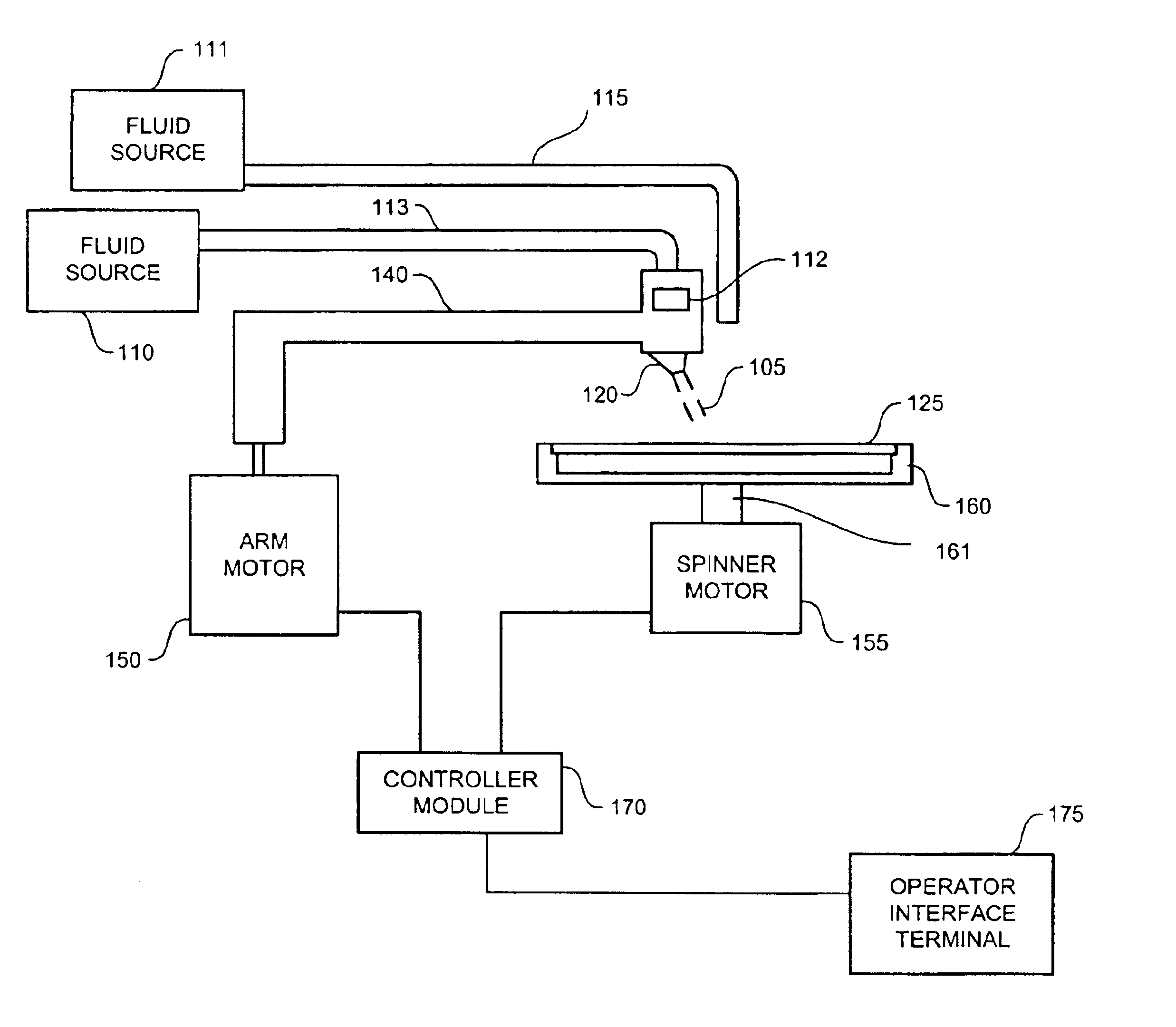
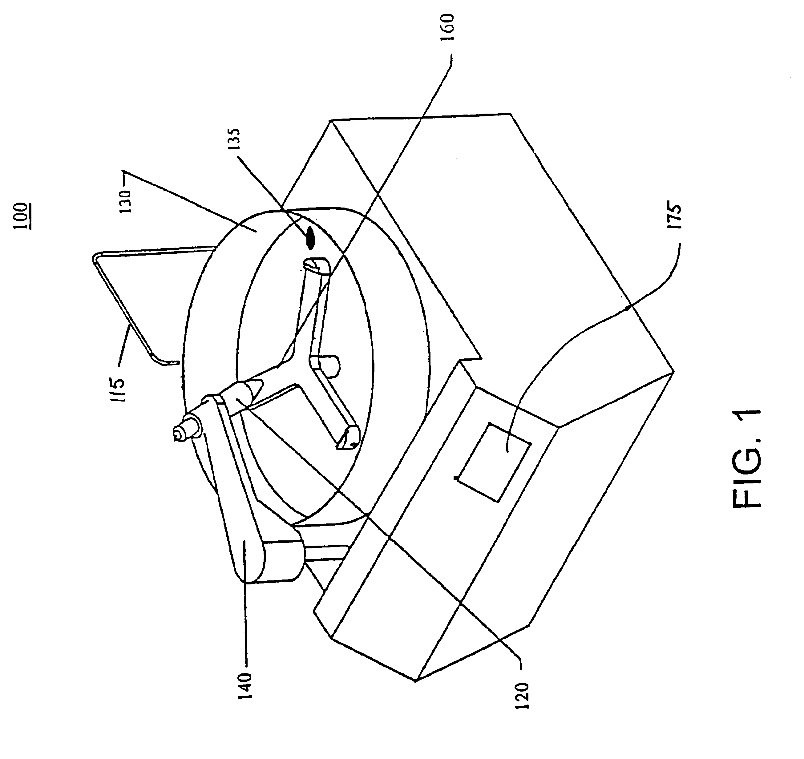
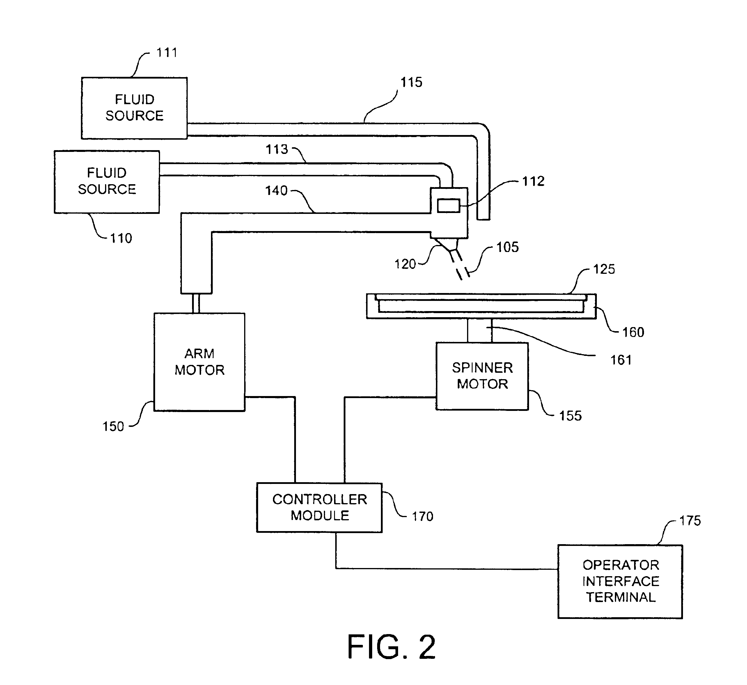
Referring to FIG. 1, a cleaning system 100 in accordance with one embodiment of the present invention is illustrated. Generally, the workpiece to be cleaned is placed in and held by the chuck 160. To remove contaminants, chuck 160 is rotated slowly while a nozzle 120 directs a stream of cleaning fluid 105 (FIG. 2) energized with megasonic energy towards the surface of the workpiece. Arm 140 moves...


PUM

PropertyMeasurementUnit
optimal angleaaaaaaaaaa
fixed distanceaaaaaaaaaa

Abstract

The present invention is directed to a method, system, and apparatus for applying megasonic energy to the surface of a workpiece for the removal of contaminants. A nozzle dispenses a stream of deionized water or other cleaning fluid at a radial position on the surface. A stepping motor moves the arm over the surface, in a step-wise manner, allowing megasonic energy to be applied in a uniform manner. The workpiece is rotated at low speeds to provide a more uniform application. Chemical solutions may optionally be added to dissolve contaminants or change the Zeta potential of the contaminants to make particles easier to detach and suspend. A high-RPM dry spin cycle further removes cleaning fluid and suspended contaminants, preventing them from reattaching. The present invention is compatible with numerous types of workpieces including 12'' semiconductor wafers.

Description

1. Field of the InventionThe present invention relates generally to the cleaning of a microelectronic workpiece. More particularly, it concerns an improved method and apparatus to remove submicron-sized contaminants from the surface of a workpiece using megasonic energy.2. Description of Related ArtIn general, at one or more stages in the semiconductor fabrication process, there is a need to clean the wafer or other microelectric workpiece to remove contaminants and other residue. Contaminants typically include films, discrete particles, particulates, micro-droplets, vapors and residue.As the design rule of semiconductor devices decreases to the submicron region, the tolerable size of the contaminants produced during the fabrication process is also decreased. Even extremely small foreign particles may cause fatal defects during the fabricating process, thereby decreasing the reliability and yield of the fabrication facility. As such, cleaning a workpiece to remove particulates and r...

Claims


Application Information

Patent Timeline
Patent Type & Authority Patents(United States)
IPC IPC(8): B08B3/02H01L21/00
CPCB08B3/02H01L21/67051Y10S134/902B08B2203/0288
Inventor KUYEL, BIROL
Owner KUYEL BIROL
Learn More