

Non-volatile semiconductor memory device
a semiconductor memory and non-volatile technology, applied in static storage, digital storage, instruments, etc., can solve the problem that writing and erasure cannot be performed
- Summary
- Abstract
- Description
- Claims
- Application Information
AI Technical Summary
Problems solved by technology
Method used
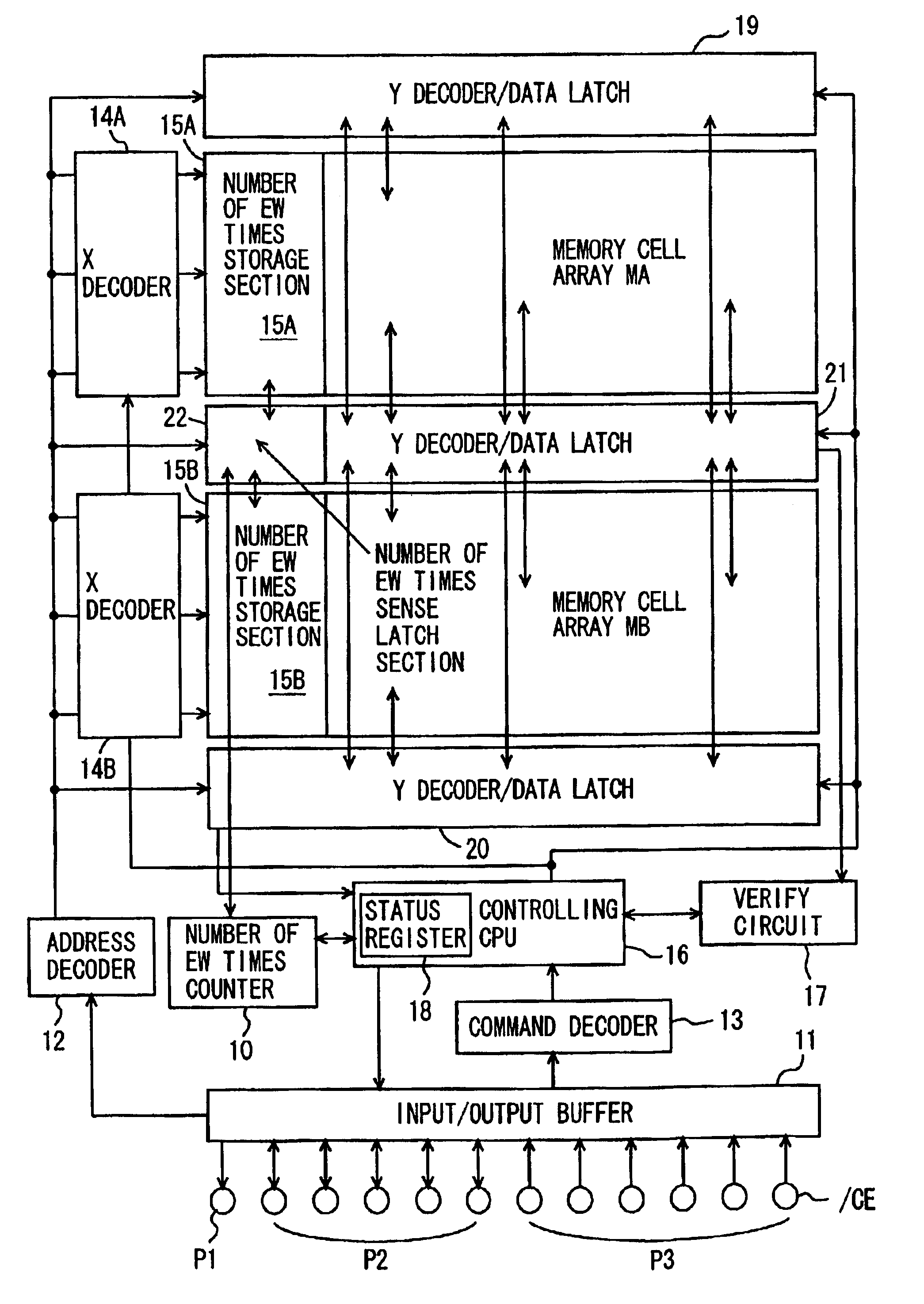
Image

Examples
second example
Pulse Setting in Consideration of Change in Data Holding Characteristics Due to Rewriting
FIG. 47 shows a relationship between a change in threshold voltage when data is held in a memory cell and the number of times of rewriting. In FIG. 47, the ordinate indicates a change amount in threshold voltage .DELTA.Vth, while the abscissa indicates the number of times of rewriting. A change amount in threshold voltage .DELTA.Vth indicates a change in threshold voltage of a memory cell when a prescribed time elapses immediately after data writing. As shown in FIG. 47, as the number of times of rewriting increases, a change amount in threshold voltage .DELTA.Vth becomes larger, and accordingly, a threshold voltage is lowered.
As for a margin for correct reading of data, as shown in FIG. 48, it is required that a margin .DELTA.M for variations in power supply voltage and temperature and the change amount in threshold voltage .DELTA.Vth are secured between lower side read voltage VRW and write ve...
first embodiment
[First Embodiment]
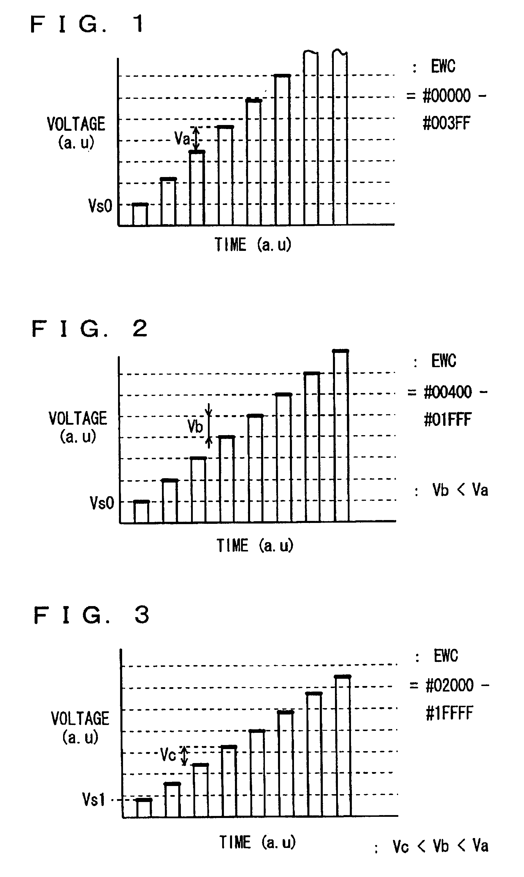
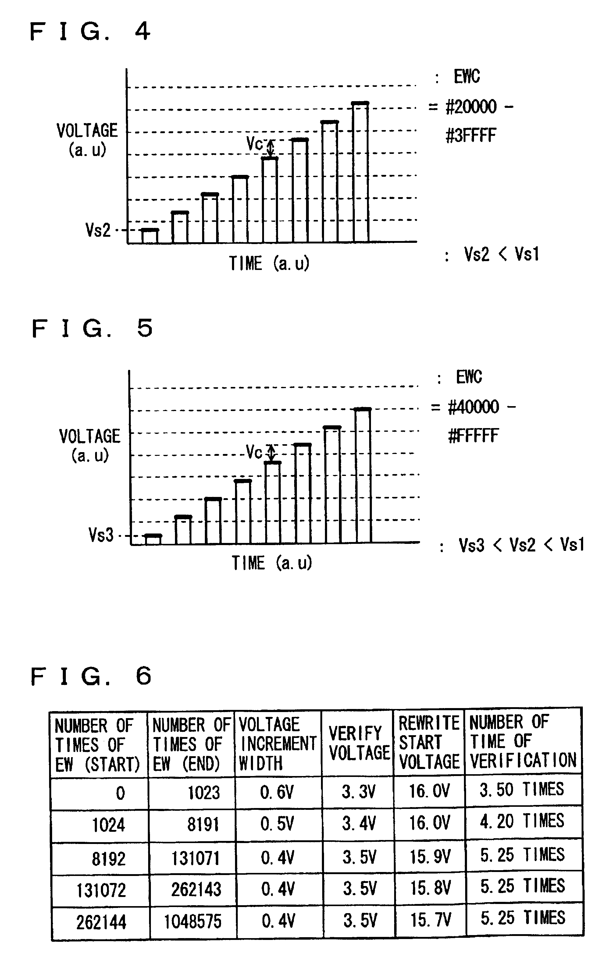
FIGS. 1 to 5 are graphs each showing setting of a write pulse series according to a first embodiment of the present invention. As shown in FIGS. 1 to 5, by performing setting of a write pulse corresponding to characteristics of a memory cell according to a number of rewriting count value EWC, a write time is reduced while maintaining reliability of a memory cell. Here, number of rewriting count value EWC indicates the number of times of rewriting stored in a number of rewriting storage section described later. In a case where rewriting to a memory cell is actually performed, an actual number of times of rewriting of the memory cell is greater by one than a number of rewriting count value EWC stored therein. In the following description, a stored number of times of rewriting is regarded as the number of rewriting count value EWC.
At an initial stage of a region from #00000 to #003FF (a region from the first writing to the 1023-rd rewriting) in the number of rewriting...
second embodiment
[Second Embodiment]
FIGS. 15 to 19 are graphs showing write pulse strings set in a non-volatile semiconductor memory device according to a second embodiment of the present invention. In the second embodiment, a write pulse width increase rate .beta. is varied instead of a change in voltage increment width of a write pulse. Moreover, a pulse width of a write start pulse applied at the first rewrite operation is altered instead of a change in voltage level of the write start voltage.
That is, as shown in FIG. 15, when the number of rewriting count value EWC is #00000 to #003FF (to the 1023-rd rewriting from the first rewriting), the write pulses are generated with a write start pulse (the first write pulse) having a pulse width of Wa and with a pulse width increase rate set to .beta.1. A voltage level of the write pulse is at a constant value. In a case where a pule width is altered, since writing is performed successively on a slower memory cell, a pulse width in a pulse series is succ...
PUM
 Abstract
Description
Claims
Application Information