

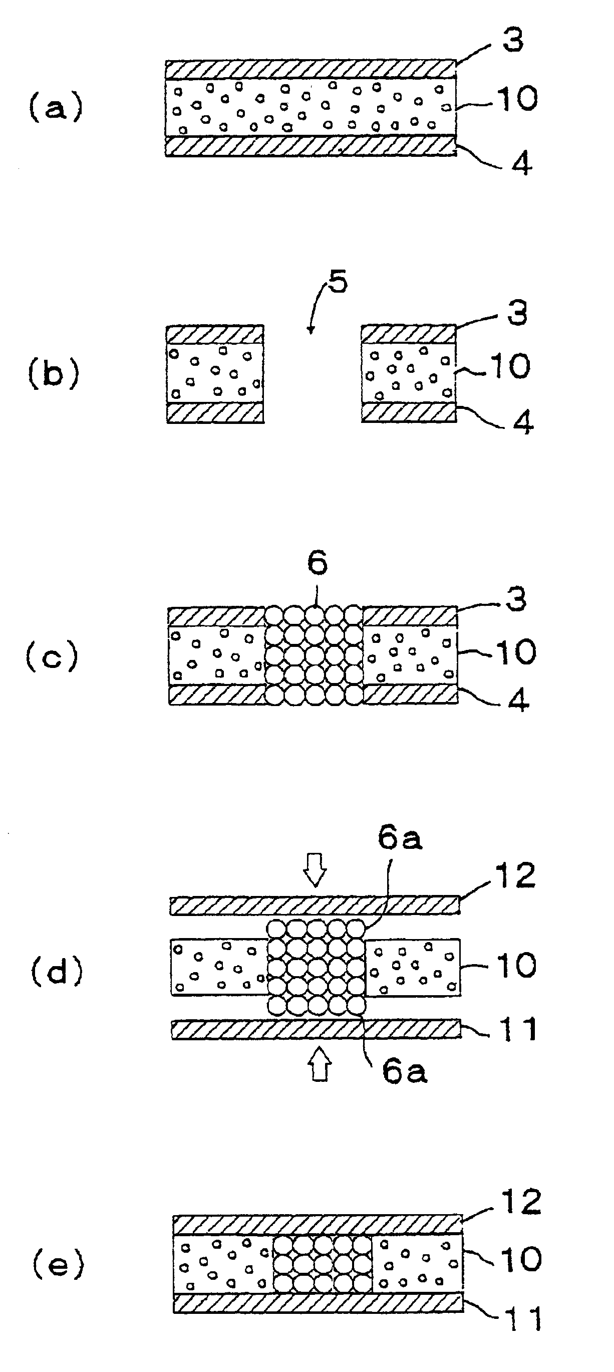
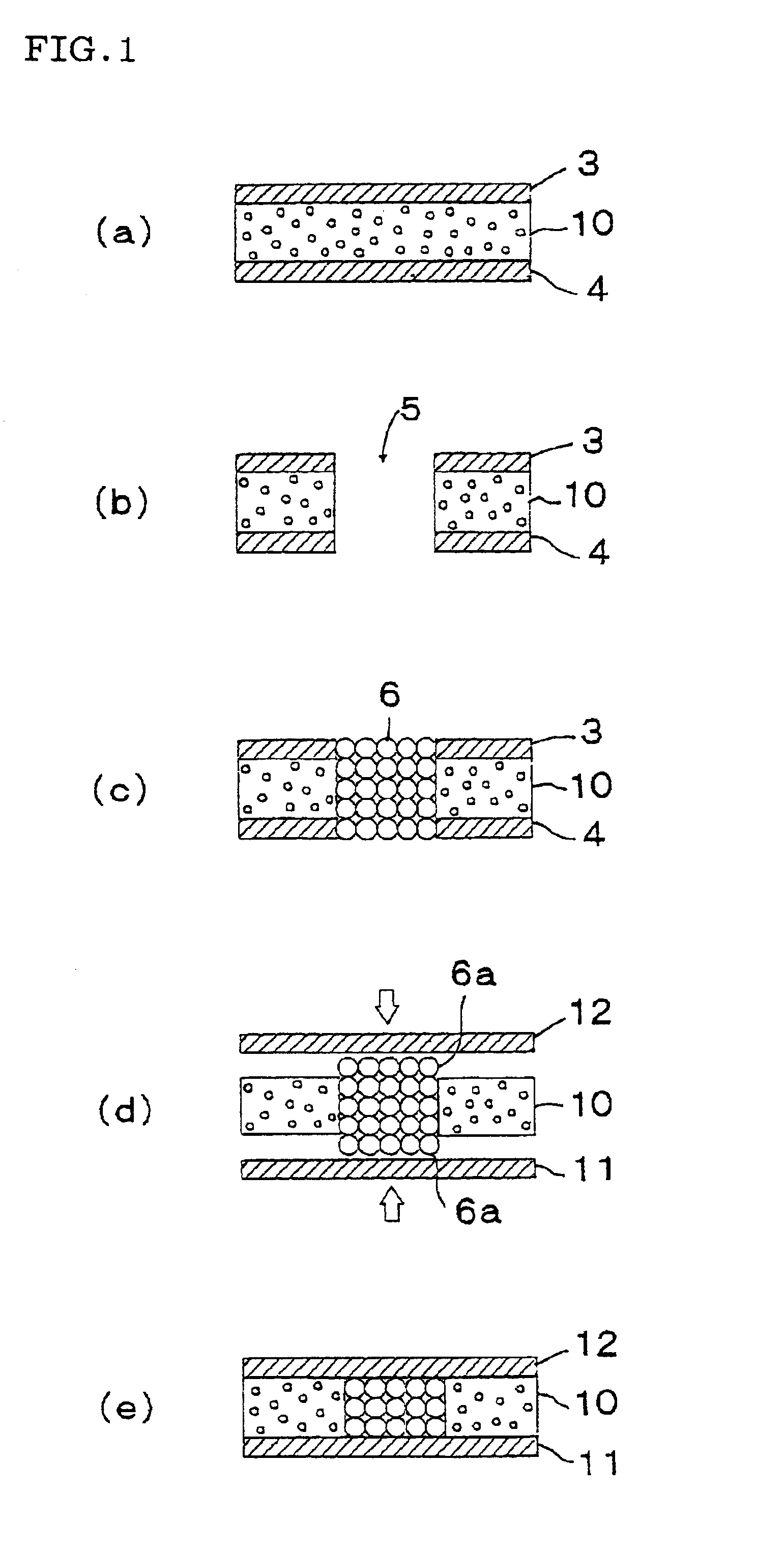
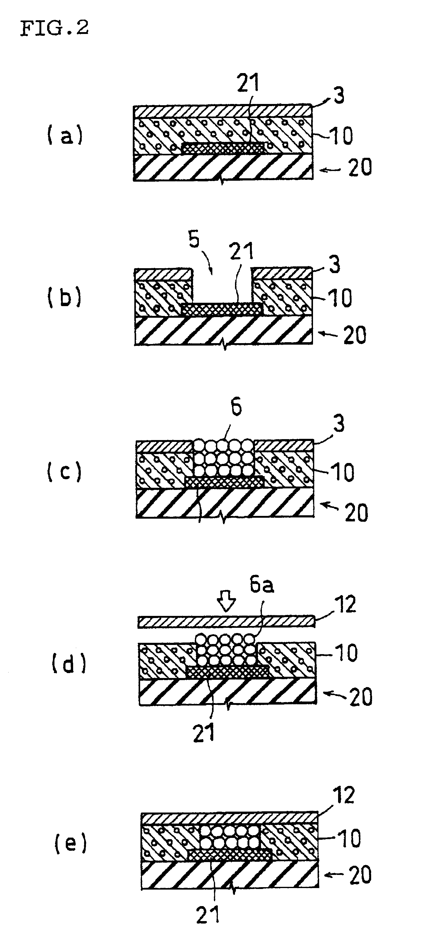
Wiring board and method of manufacturing the same
a manufacturing method and technology of wiring board, applied in the direction of resistive material coating, surface pretreatment, adhesive processes, etc., can solve the problems of difficult to produce thin and uniform woven and nonwoven fabrics, the workability of through holes is apt to be deteriorated by fibers constituting nonwoven fabrics, and the thickness of a layer is limited
- Summary
- Abstract
- Description
- Claims
- Application Information
AI Technical Summary
Benefits of technology
Problems solved by technology
Method used
Image

Examples
example 1
A hexane solution of isophthalic chloride and an m-phenylene diamine aqueous solution were caused to react equimolarly so that aromatic polyamide was obtained. The aromatic polyamide (precipitate) was repeatedly washed by water and alcohol and water and was then dried in vacuum overnight at 60.degree. C. so that a dry polymer was obtained. The polymer was dissolved in N-methyl-2-pyrrolidone (NMP), and furthermore, polyvinyl pyrrolidone (PVP) (manufactured by ISP JAPAN CO., LTD., K-90) and water were mixed so that a polymer solution (film forming solution) containing aromatic polyamide (100 parts by weight), NMP (900 parts by weight), PVP (40 parts by weight) and water (40 parts by weight) was obtained.
A PEN film having a thickness of 12 .mu.m (manufactured by TEIJIN LIMITED, Teonex film) was coated with the solution in a thickness of 30 .mu.m, and was immersed in a water tank at 60.degree. C. to form a porous film. Furthermore, the film was preserved for twenty-four hours to elimina...
PUM
| Property | Measurement | Unit |
|---|---|---|
| porosity | aaaaa | aaaaa |
| thickness | aaaaa | aaaaa |
| mean pore diameter | aaaaa | aaaaa |
Abstract
Description
Claims
Application Information