Synchronous semiconductor memory device and method of processing data thereof

a semiconductor memory and data processing technology, applied in the field of synchronous semiconductor memory devices and methods of processing data thereof, can solve the problems of complicated circuit configuration and inability to operate at a high enough speed of double data rate semiconductor memory devices

Inactive Publication Date: 2004-07-13
SAMSUNG ELECTRONICS CO LTD
View PDF2 Cites 20 Cited by
  • Summary
  • Abstract
  • Description
  • Claims
  • Application Information

AI Technical Summary

Problems solved by technology

However, in a system requiring very high-speed operation, even the double data rate semiconductor memory device cannot operate at a high enough speed.
However, the conventional synchronous semiconductor memory device having a 4-bit pre-fetch mode has a problem in that its circuit configuration is complicated.

Method used


Image

  • Synchronous semiconductor memory device and method of processing data thereof
  • Synchronous semiconductor memory device and method of processing data thereof
  • Synchronous semiconductor memory device and method of processing data thereof

Examples


Embodiment Construction

Reference will now be made in detail to preferred embodiments of the present invention, example of which is illustrated in the accompanying drawings.

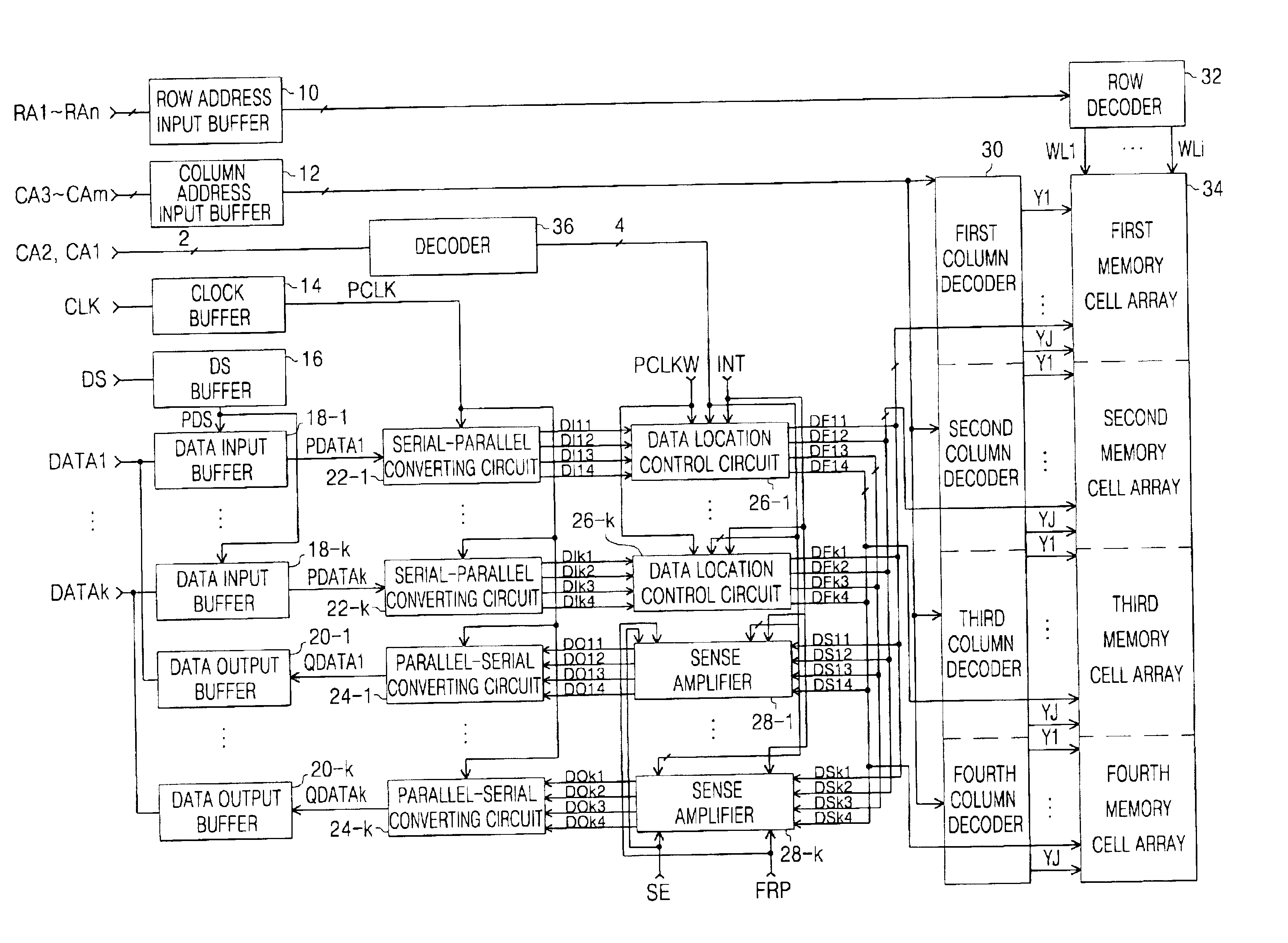
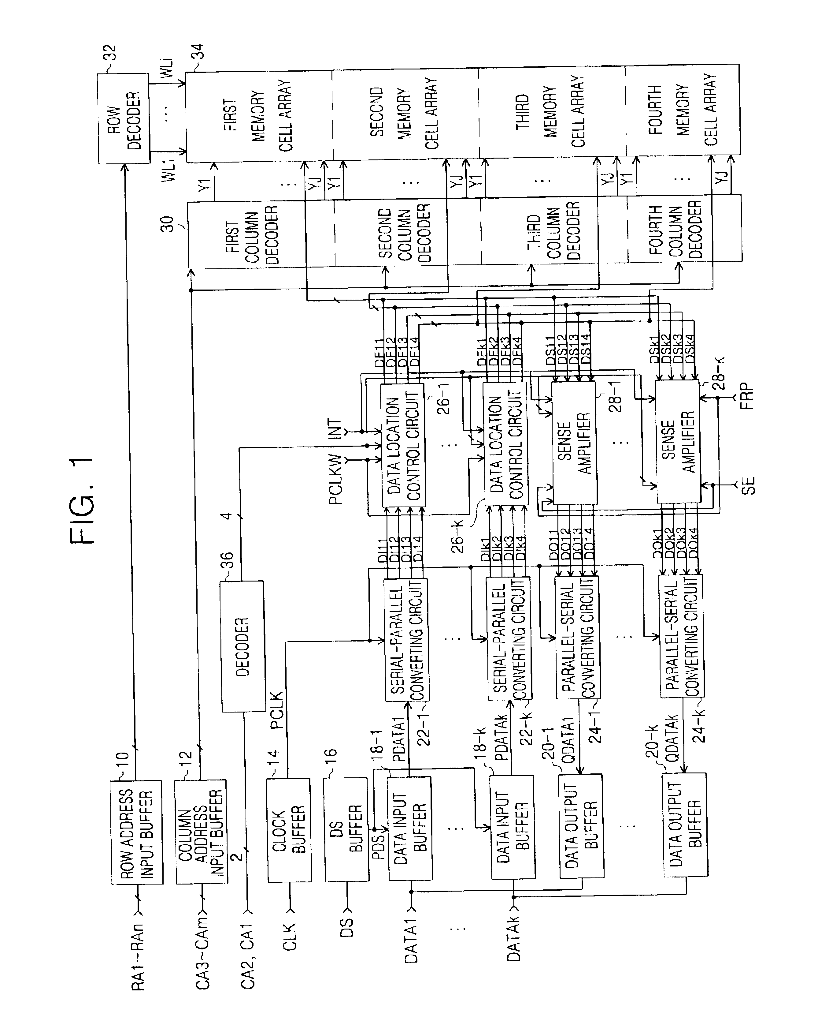
FIG. 1 is a block diagram illustrating a synchronous semiconductor memory device having a 4-bit pre-fetch mode according to an embodiment of the present invention.

The synchronous semiconductor memory device having a 4-bit pre-fetch mode of FIG. 1 includes a row address input buffer 10, a column address buffer 12, a clock buffer 14, a DS buffer 16, data input buffers 18-1 to 18-k, data output buffers 20-1 to 20-k, serial-parallel converting circuits 22-1 to 22-k, parallel-serial converting circuits 24-1 to 24-k, data location control circuits 26-1 to 26-k, sense amplifiers 28-1 to 28-k, a column decoder 30, a row decoder 32, a memory cell array 34, and a decoder 36. The memory cell array 34 includes first to fourth memory cell arrays. The column decoder 30 includes first to fourth column decoders.

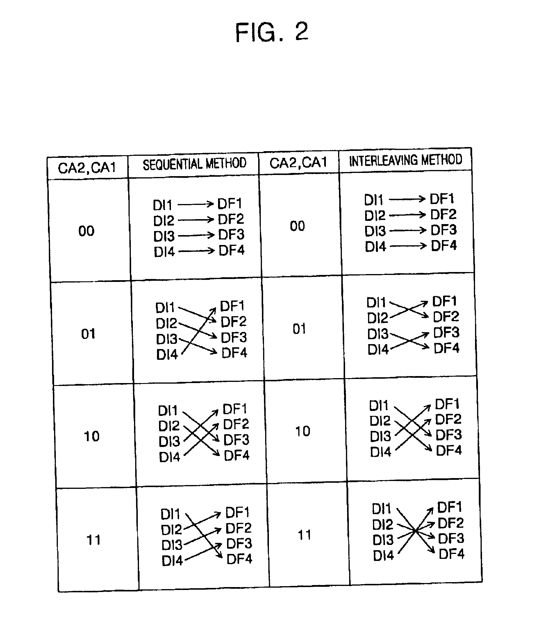
Operation of the synchronous semiconducto...


PUM


Abstract

The present invention involves a synchronous semiconductor memory device having a 4-bit prefetch mode a method of processing a data thereof, comprising first to fourth memory cell arrays each having memory cells, a serial-parallel converting means converting a plurality of 4-bit data serially applied during a write operation into a plurality of 4-bit parallel data, a data loation control means location-controlling and outputting each of the plurality of the 4-bit parallel data output from the serial-parallel converting means in response first to fourth decoding signals generated by decoding the 2-bit column address to the first to fourth memory cell arrays, by a sequential method or by an interleaving method, during the write operation, a sense amplifier amplifying a plurality of 4-bit data output from each of the first to fourth memory cell arrays, and location-controlling and outputting them in response the first to fourth decoding signals, by a sequential method or by an interleaving method, during a read operation, and a parallel-serial converting means converting and outputting a plurality of 4-bit parallel data output from the sense amplifier during a read operation into a plurality of 4-bit serial data, whereby the circuit configuration is simple.

Description

This application claims benefit and priority of Korean Patent Application No. 2001-43549, filed on Jul. 19, 2001, under 35 U.S.C. .sctn.119, the entirety of which is hereby incorporated by reference.1. Field of the InventionThe present invention relates to a semiconductor memory device, and more particularly, to a synchronous semiconductor memory device having a 4-bit pre-fetch mode and a method of processing data thereof.2. Description of Related ArtA synchronous semiconductor memory device has widely been used as a main memory in various industrial fields such as a desk-top computer system or a portable computer system. Such synchronous semiconductor memory devices include single data rate synchronous semiconductor memory devices and double data rate synchronous semiconductor memory devices.The single data rate synchronous semiconductor memory device receives a datum at a rising edge of a clock signal. The double data rate synchronous semiconductor memory device receives two data ...

Claims


Application Information

Patent Timeline
Patent Type & Authority Patents(United States)
IPC IPC(8): G11C7/10G11C11/4096
CPCG11C7/1006G11C7/1042G11C7/1051G11C7/1066G11C7/1072G11C7/1078G11C2207/107G11C11/4096
Inventor LA, ONE-GYUN
Owner SAMSUNG ELECTRONICS CO LTD
Why Eureka
Try Eureka