Dynamic threshold voltage MOS transistor fitted with a current limiter

a current limiter and threshold voltage technology, applied in the direction of electric variable regulation, electric pulse generator, automatic control of pulses, etc., can solve the problems of limiter transistor and the connection with the first transistor being incompatible with the requirements for reducing the size of components, the electrical diagram of the device mentioned above cannot be directly integrated in a version, and the integration density of components is ever greater

Inactive Publication Date: 2004-09-07
COMMISSARIAT A LENERGIE ATOMIQUE ET AUX ENERGIES ALTERNATIVES
View PDF19 Cites 52 Cited by
  • Summary
  • Abstract
  • Description
  • Claims
  • Application Information

AI Technical Summary

Benefits of technology

The effect of the fourth zone is thus to extend one of the second or thir

Problems solved by technology

Such a device is however little used on account of the significant increase in static current related to the operation of the bipolar component.
One essential difficulty related to the manufacture of a device according to the diagrams in FIG. 2 or 3 lies in the fact that making the limiter transistor and the

Method used


Image

  • Dynamic threshold voltage MOS transistor fitted with a current limiter
  • Dynamic threshold voltage MOS transistor fitted with a current limiter
  • Dynamic threshold voltage MOS transistor fitted with a current limiter

Examples


Embodiment Construction

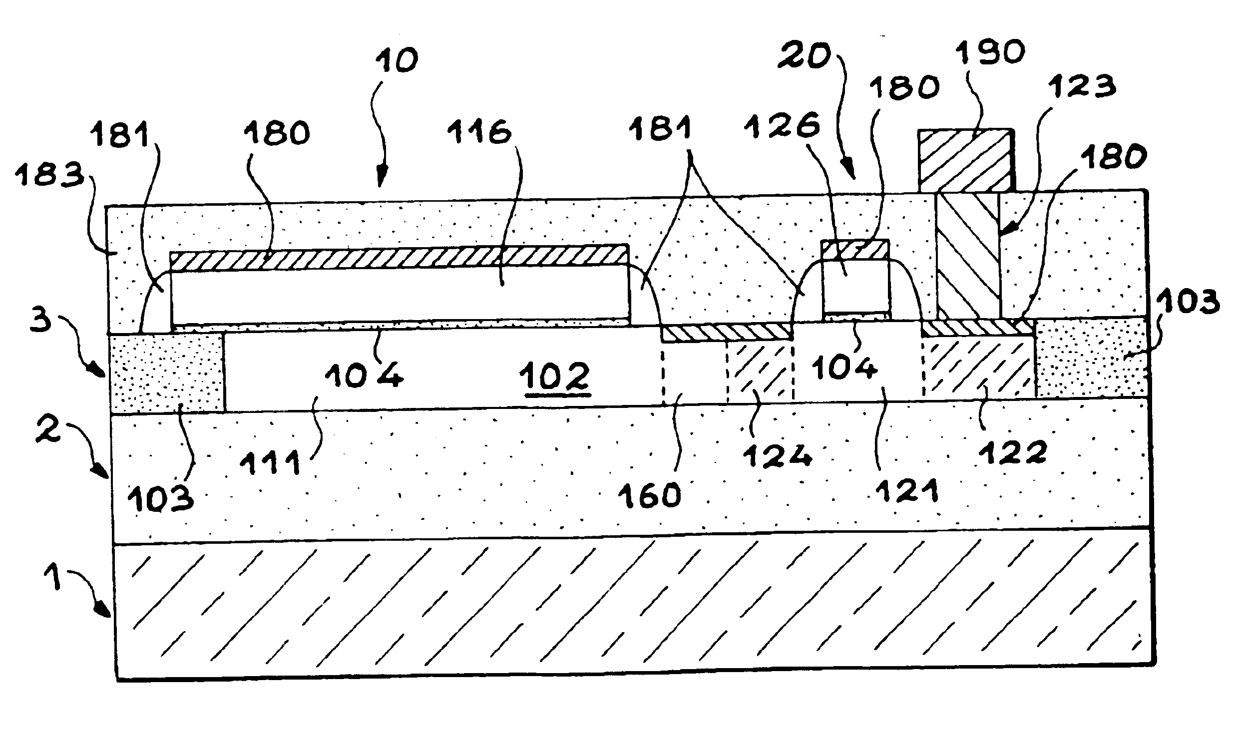
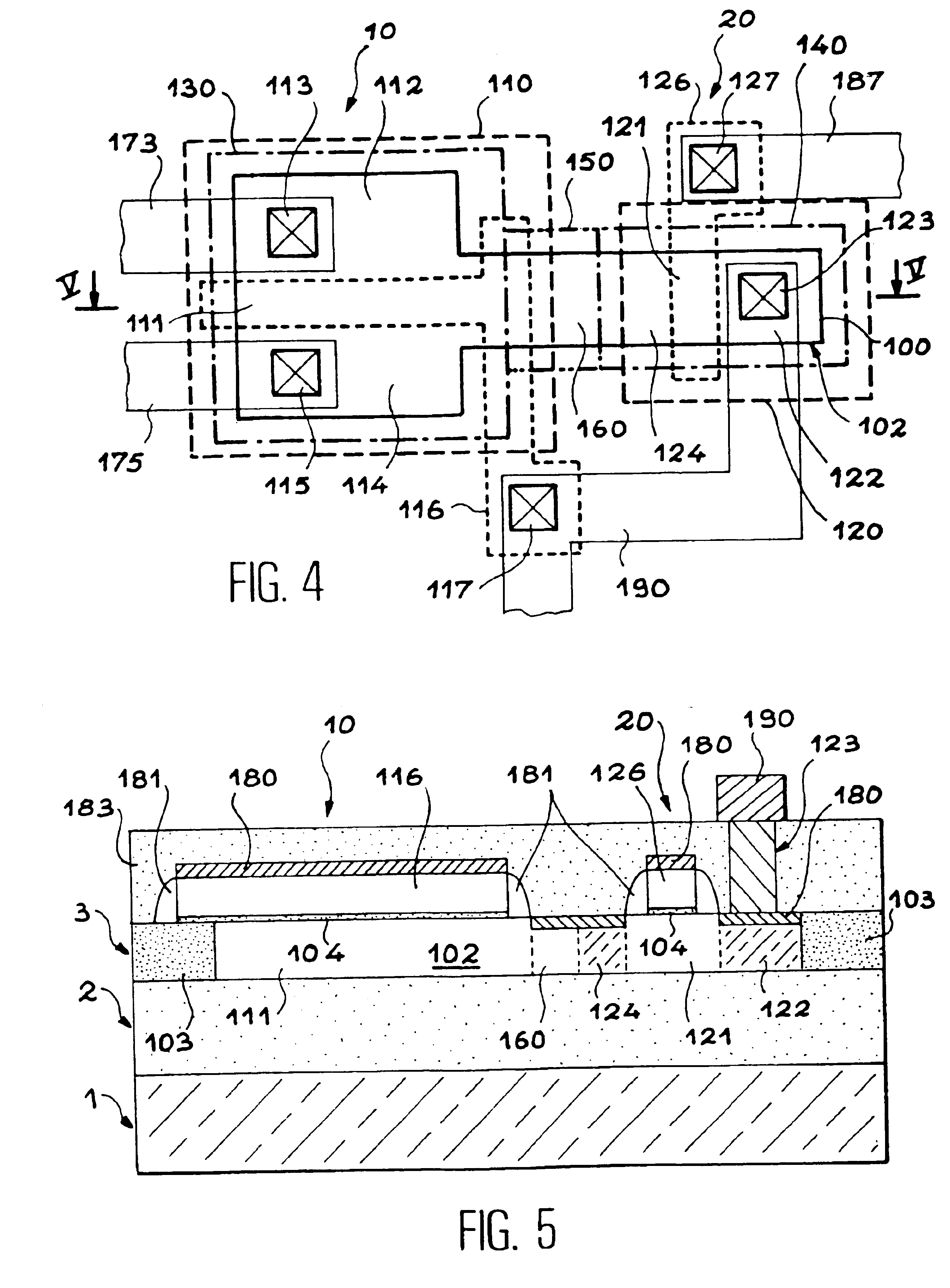
The following description refers to the manufacture of the device in the silicon surface layer of an SOI type substrate.

The plane of FIG. 4 corresponds to a view from above of the device according to a first embodiment.

A continuous line 100 in FIG. 4 represents the limit of the active zone 102 defined on the surface layer of silicon.

Outside the zone defined by the line 100, the surface layer of silicon is oxidised so as to isolate the active zone laterally.

A certain number of impurity implantation ranges defined above the active zone, and described in more detail hereinafter, partly overlap the oxidised silicon, for implantation pattern design reasons. However, it should be noted that the implanted doping impurities reaching the silicon oxide which surrounds the active zone, are ineffective and do not modify the isolating electrical character of the oxide.

At least one first P-type implantation is practised in two implantation ranges 110, 120, which correspond in particular to the ch...


PUM


Abstract

The invention concerns a semi-conductor device comprising on a substrate:a first dynamic threshold voltage MOS transistor (10), with a gate (116), and a channel (111) of a first conductivity type, anda current limiter means (20) connected between the gate and the channel of said first transistor.In accordance with the invention, this first transistor is fitted with a first doped zone (160) of the first conductivity type, connected to the channel, and the current limiter means comprises a second doped zone (124) of a second conductivity type, placed against the first doped zone and electrically connected to the first zone by an ohmic connection.Application to the manufacture of CMOS circuits.

Description

This invention concerns a dynamic threshold voltage MOS transistor (insulated gate Transistor) fitted with an integrated current limiter. This device is intended in particular to be made on an SOI (silicon on insulator) type substrate, in other words a substrate having a thin surface layer of silicon insulated by an underlying layer of oxide.The invention also concerns a process for making such a device in a particularly compact form with a view to integrating it into a circuit.The invention finds applications particularly in the manufacture of CMOS circuits operating with very low supply voltages such as for example micro-processors or digital signal processors (DSP).PRIOR ARTThe prior art is shown particularly in documents (1), (2), (3) and (4) mentioned below and the references for which are given at the end of this description.A usual MOS transistor may be considered as being made up of two intrinsic components. The first component is the MOS transistor itself, in which the curr...

Claims


Application Information

Patent Timeline
IPC IPC(8): H01L27/12H01L21/70H01L21/84H01L27/06H01L27/08H01L29/786
CPCH01L21/84H01L27/1203Y10S257/903Y10S257/904
Inventor PELLOIE, JEAN-LUC
Owner COMMISSARIAT A LENERGIE ATOMIQUE ET AUX ENERGIES ALTERNATIVES
Why Eureka
Try Eureka