Integrated circuits protected against reverse engineering and method for fabricating the same using vias without metal terminations

a technology of integrated circuits and vias, which is applied in the direction of electrical equipment, semiconductor devices, semiconductor/solid-state device details, etc., can solve the problems of difficult reverse engineering determination, increased cost and time consumption of reverse engineering, and unpredictable use of vias to provide connections between metal layers to achieve secure circuits.

Inactive Publication Date: 2004-09-14
HRL LAB
View PDF105 Cites 38 Cited by
  • Summary
  • Abstract
  • Description
  • Claims
  • Application Information

AI Technical Summary

Benefits of technology

This invention makes the use of vias to provide connections between metal layers unpredictable and difficult to be determined accurately. Hence, the circuit will appear to be one thing, while in fact it is something else. This is a good way to prevent reverse engineering.
Such non-metal terminating vias will make it very difficult for a reverse engineer to determine what the signal routing pattern really is, making the process of reverse engineering more expensive and time consuming effectively rendering the circuit secure from such intrusion.

Problems solved by technology

This invention makes the use of vias to provide connections between metal layers unpredictable and difficult to be determined accurately.
Such non-metal terminating vias will look like an interconnection between adjacent metal layers / lines to the reverse engineer, but they in fact provide no such interconnection.
Such non-metal terminating vias will make it very difficult for a reverse engineer to determine what the signal routing pattern really is, making the process of reverse engineering more expensive and time consuming effectively rendering the circuit secure from such intrusion.

Method used


Image

  • Integrated circuits protected against reverse engineering and method for fabricating the same using vias without metal terminations
  • Integrated circuits protected against reverse engineering and method for fabricating the same using vias without metal terminations

Examples


Embodiment Construction

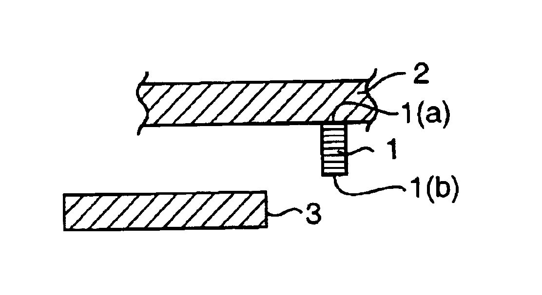
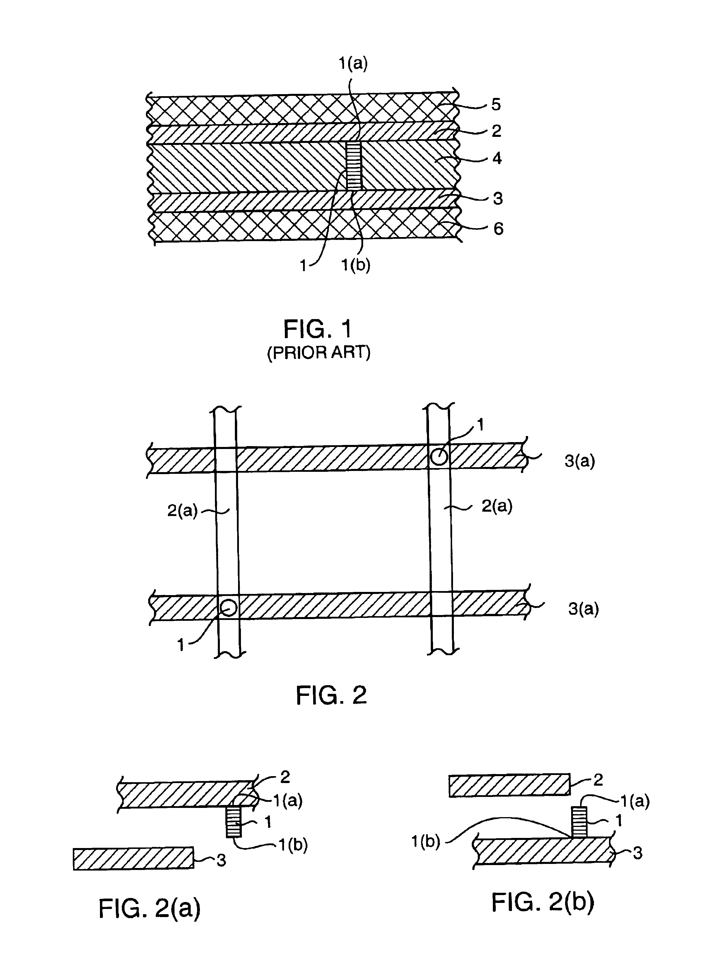
FIG. 1 shows a usual via 1 connecting an upper metal layer 2 and a lower metal layer 3. The via 1 has two ends: a first end 1(a) and a second end 1(b). The upper and lower metal layers are separated by an insulating layer 4, typically made of silicon oxide. Insulating layers 5 and 6, typically, occur above and below metal layers 2 and 3. The insulating layers 4, 5 and 6 are disposed in a semiconductor device, preferably, an integrated circuit (not shown). The via 1 is filled with a metal, typically the same metal as the metal of metal layers 2 and 3, this metal usually being tungsten.

FIG. 2 shows that metal lines 2(a) and 3(a), within the two metal layers 2 and 3, respectively, do not typically run parallel. They are disposed in parallel planes, but the signal metal lines 2(a) and 3(a) are not parallel. Instead, the metal pattern, when viewed from the top, as shown on FIG. 2, is usually two arrays of lines proceeding in orthogonal directions, when viewed as projected onto a single p...


PUM


Abstract

A device adapted to protect integrated circuits from reverse engineering comprising a part looking like a via connecting two metal layers, but in fact attached only to one metal layer and spaced from the other. Having such "trick" via would force a reverse engineer to think there is a connection where there is none. A method for fabricating such device.

Description

I. BACKGROUND OF THE INVENTION1. Field of the InventionThis invention relates to the field of the prevention of reverse engineering of integrated circuits and / or making such reverse engineering so difficult and time-consuming as to make reverse engineering of integrated circuits non-feasible.More particularly, this invention relates to using, in order to prevent and / or discourage such reverse engineering, vias (i.e., holes etched in the oxide layers between metal layers and then filled with metal to affect a connection between metal layers) either not beginning on a metal layer or not terminating on a metal layer.2. Description of the Related ArtThe design and development of semiconductor integrated circuits require a thorough understanding of the complex structures and processes and involve many man-hours of work requiring high skill, costing considerable sums of money.In order to avoid this time and effort, some developers resort to the practice of reverse engineering, disassembli...

Claims


Application Information

Patent Timeline
Patent Type & Authority Patents(United States)
IPC IPC(8): H01L23/58H01L23/52H01L23/522H01L27/02
CPCH01L23/5226H01L23/573H01L27/0203Y10S438/926H01L2924/0002H01L2924/00
Inventor CHOW, LAP-WAIBAUKUS, JAMES P.CLARK, JR., WILLIAM M.
Owner HRL LAB
Why Eureka
Try Eureka