Method of forming metal wire of semiconductor device

a metal wire and semiconductor technology, applied in semiconductor devices, semiconductor/solid-state device details, electrical devices, etc., can solve the problems of deterioration of electrical properties of devices, increased contact resistance, and difficulty in adequately filling contact holes in metal contact process, so as to reduce junction leakage current, improve the reliability of semiconductor devices, and achieve maximum

Inactive Publication Date: 2004-09-28
SK HYNIX INC
View PDF5 Cites 11 Cited by
  • Summary
  • Abstract
  • Description
  • Claims
  • Application Information

AI Technical Summary

Benefits of technology

Therefore, methods of forming metal wires or contact of semiconductor devices are disclosed which reduces the junction leakage current caused by the reduction of the current resistance and which improves the reliability of the semiconductor device by maximally depressing the diffusion of the dopant in the junction area consumed through heat treatment in the formation of the titanium silicide film and further which improves the contact resistance caused by the increase of the concentration of the dopant existing in the junction area.

Problems solved by technology

Therefore, it becomes difficult to adequately fill the contact hole in metal contact process.
Thus the contact resistance is increased and the electrical properties of the device are deteriorated.
However, the more the device is integrated, the smaller the concentration of ions existing in the junction area.
This generates an additional problem increased contact resistance.

Method used


Image

  • Method of forming metal wire of semiconductor device
  • Method of forming metal wire of semiconductor device
  • Method of forming metal wire of semiconductor device

Examples


first embodiment

FIGS. 2a to 2c are cross-sectional views showing a method of forming a metal wire of a semiconductor device according to a

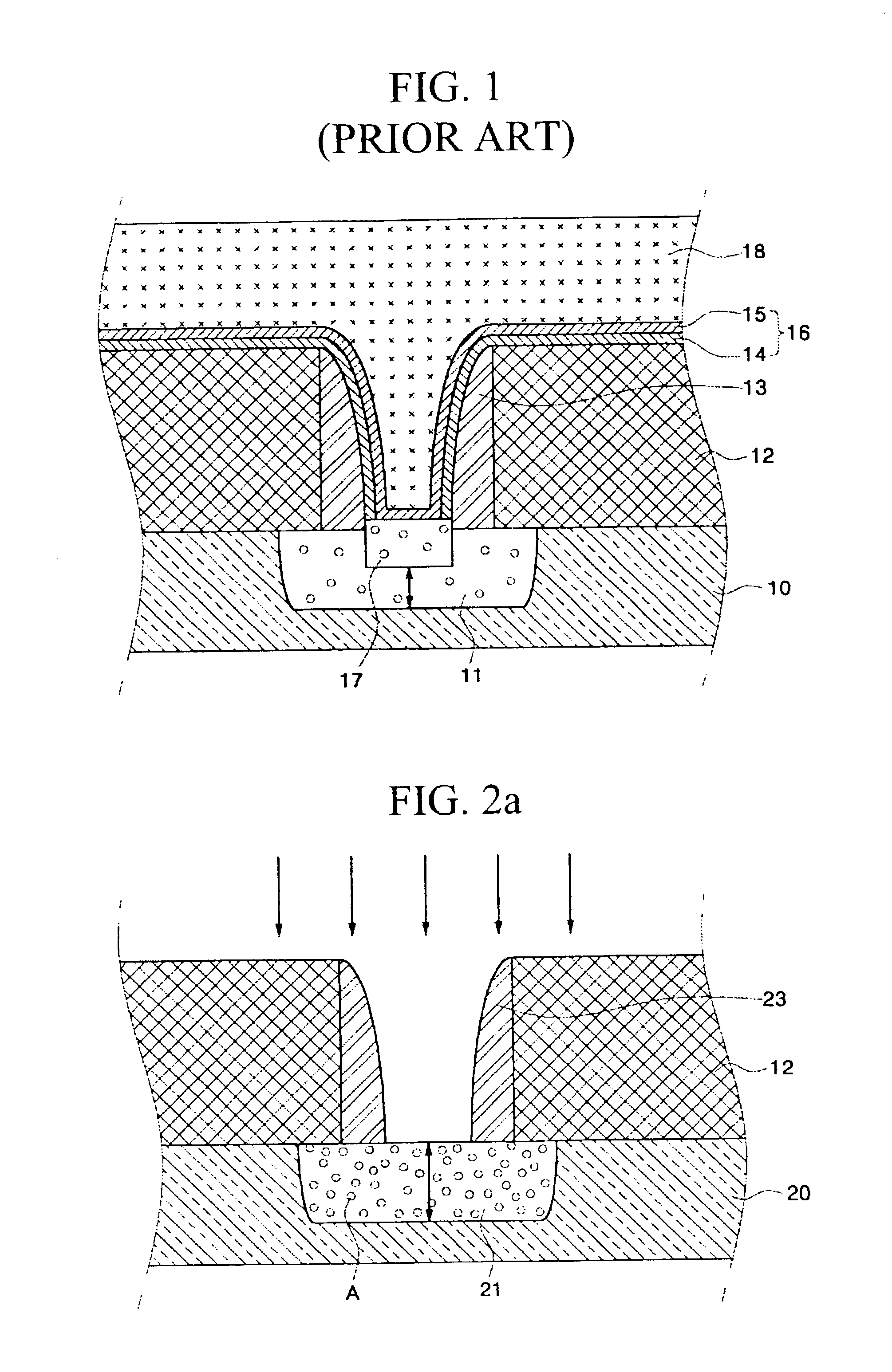
Firstly, as illustrated in FIG. 2a, a junction area 21 is formed on a semiconductor substrate 20 by carrying out plasma treatment using a B.sub.2 H.sub.6 gas in a CVD chamber. At this time, the dopant (A) (for instance, B.sup.+ generated from the B.sub.2 H.sub.6 gas) is included in the junction area 21.

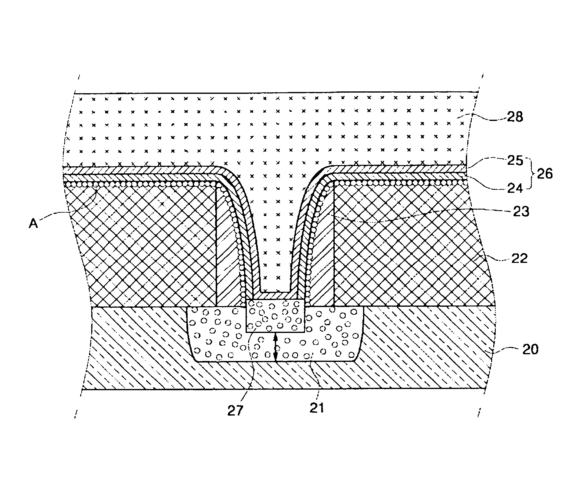
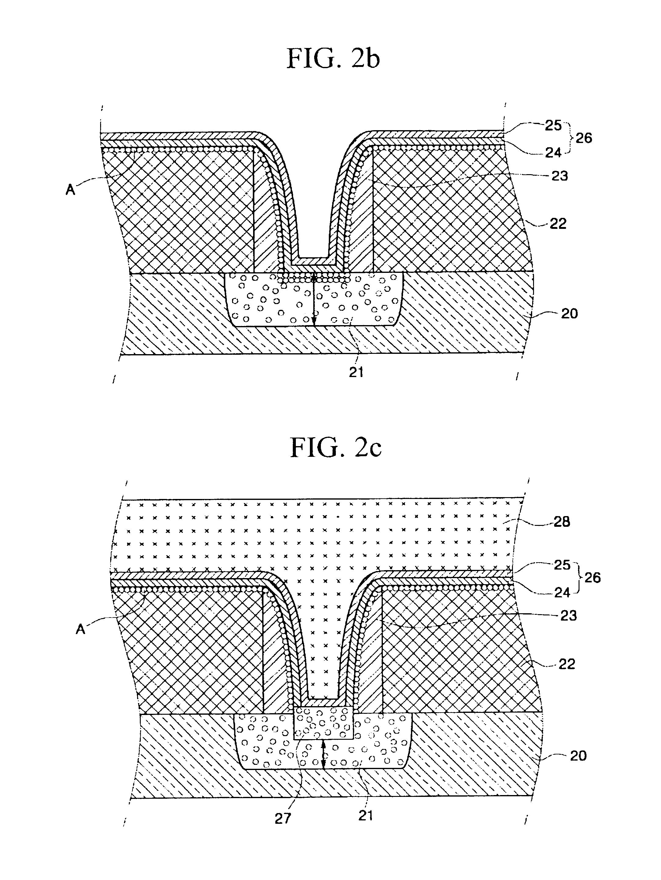
Next, an interlayer insulating film 22 is formed on the semiconductor substrate 20 in which the junction area 21 is formed. A contact hole is formed by etching a selected portion of the interlayer insulating film 22 to expose the junction area 21. Next, for electrical insulation with peripheral devices, a spacer insulating film 23 is formed on a side wall of the contact hole.

Next, plasma treatment is carried out using a B.sub.2 H.sub.6 gas in a CVD chamber to add the same dopant as that of the junction area 21. At this time, it is preferred that the B.sub.2 H.sub.6...

second embodiment

Referring to FIG. 3, a method of forming a metal wire of a semiconductor device will now be described.

FIGS. 3a to 3e are cross-sectional views showing a method of forming a metal wire of a semiconductor device according to the second embodiment. The same drawing reference numerals are used for the same elements as those in the first embodiment illustrated in FIGS. 2a to 2c.

In the second embodiment, in order to maximize the depression of the diffusion of the dopant in the junction area consumed through heat treatment in the formation of the titanium silicide film to improve the contact resistance caused by the increase of the concentration of the dopant existing in the junction area, a method of adding the same dopant as that of a lower junction layer before the formation of a titanium nitride film is illustrated.

As illustrated in FIG. 3a, a junction area 21 is formed on a semiconductor substrate 20 by carrying out plasma treatment using B.sub.2 H.sub.6 gas in a CVD chamber. At this...


PUM

PropertyMeasurementUnit
temperatureaaaaaaaaaa
junction areaaaaaaaaaaa

Abstract

A method of forming a metal wire of a semiconductor device is disclosed. The method of forming a metal wire of a semiconductor device can reduce the junction leakage current caused by the reduction of the current resistance and can improve the reliability of the semiconductor device by adding the same dopant as that of a lower junction layer on the surface of a bit line contact before the deposition of the titanium film or the titanium nitride film, in order to maximize the diffusion of the dopant in the junction area consumed through heat treatment in the formation of the titanium silicide film and improve the contact resistance caused by the increase of the concentration of the dopant existing in the junction area.

Description

1. Technical FieldMethods of forming metal wires of semiconductor devices are disclosed, and more particularly, methods of forming such metal wires which can reduce junction leakage current caused by a reduction of the current resistance and can improve the reliability of the semiconductor device by adding the same dopant as that of a lower junction layer on the surface of a bit line contact before the deposition of the titanium film or the titanium nitride film. As a result, the diffusion of the dopant in the junction area consumed through heat treatment in the formation of the titanium silicide film is maximized and the contact resistance caused by the increase in the concentration of the dopant in the junction area is improved.2. Description of the Related ArtGenerally, as the integration of a semiconductor device increases, the depth of a junction area and the size of the contact hole decrease. Therefore, it becomes difficult to adequately fill the contact hole in metal contact ...

Claims


Application Information

Patent Timeline
Patent Type & Authority Patents(United States)
IPC IPC(8): H01L21/285H01L21/70H01L21/02H01L21/768H01L21/28H01L21/22H01L21/265H01L21/3205H01L23/52
CPCH01L21/28518H01L21/76802H01L21/76831H01L21/76843H01L21/76855H01L21/28
Inventor JANG, HYUN-JINYOON, JONG-YOON
Owner SK HYNIX INC
Why Eureka
Try Eureka