Semiconductor package and method for fabricating the same

a technology of semiconductor and package, applied in the direction of semiconductor/solid-state device details, semiconductor devices, electrical apparatus, etc., can solve the problems of limited mounting density, large package thickness, and inability to meet the desire of conventional semiconductor packages

Inactive Publication Date: 2004-09-28
AMKOR TECH SINGAPORE HLDG PTE LTD
View PDF77 Cites 139 Cited by
  • Summary
  • Abstract
  • Description
  • Claims
  • Application Information

AI Technical Summary

Problems solved by technology

Furthermore, in a case where the semiconductor chip 2' disposed in the opening of the circuit board 20' is a memory chip, such as a flash memory chip, SRAM chip or the like, since a plurality of semiconductor packages 100' must be mounted on a motherboard (not shown), there occurs a problem in which the mounting density is limited.
However, the desire is not satisfied by the conventional semiconductor package.
Accordingly, the package is very thick which is contrary to recent trends.
Additionally, since the height difference between the input / output pads and the circuit board is excessively enlarged, the loop height of the connection means, such as conductive wires that connect the second semiconductor chip to the circuit pattern, tends to be enlarged.
Accordingly, since the loop angle becomes an acute angle, the sweeping phenomenon of the conductive wires occurs easily by the filling pressure during a molding process, thereby causing the inferiority of the package.
However, in the conventional composite stack type semiconductor package 102', since projected pads are formed on the periphery of the circuit board of the BGA package 103' and solder balls are fusion-welded on the projected pads, the semiconductor package causes inconvenience in having an extra step to form the projected pads, and has a limitation on the reduction of the thickness of electronic devices owing to the thickness of the projected pads.
Additionally, in each of BGA packages, since a single chip is mounted in each package, there occur limitations on the maximization of the memory capacity of each package and the increase of the mounting density of each package.

Method used


Image

  • Semiconductor package and method for fabricating the same
  • Semiconductor package and method for fabricating the same
  • Semiconductor package and method for fabricating the same

Examples


first embodiment

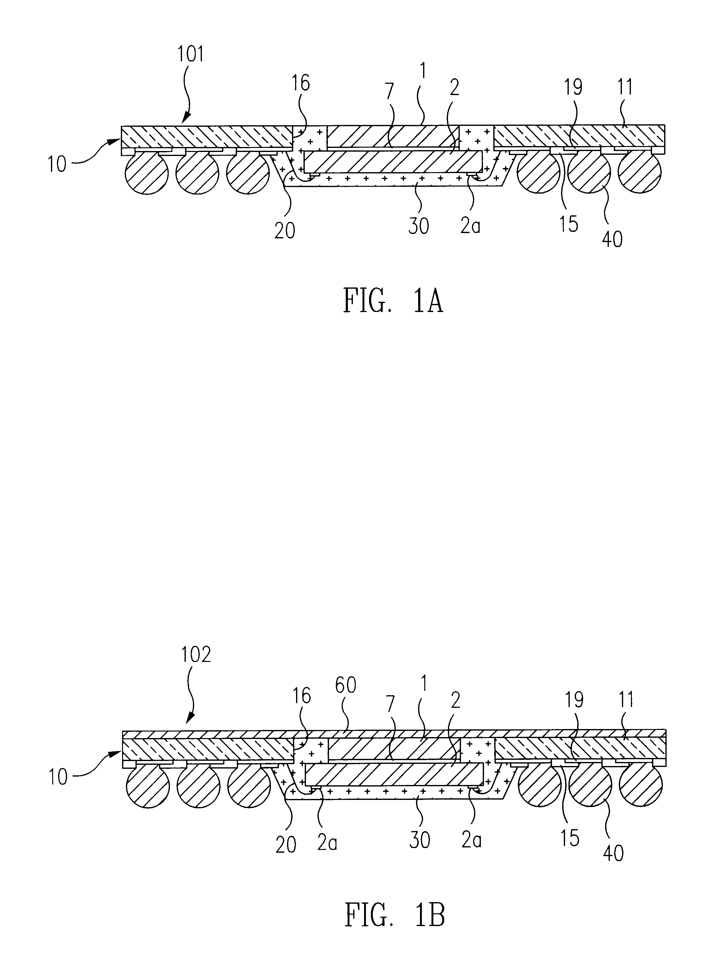
FIGS. 1A and 1B are cross sections showing semiconductor packages 101 and 102 in accordance with the present invention. In the drawings, reference numeral 1 designates a first semiconductor chip 1 on the lower surface of which input / output pads (not shown) are formed. A second semiconductor 2 is bonded on the surface on which the input / output pads are formed with a bonding layer 7 interposed between the first and second semiconductor chips 1 and 2. The bonding layer 7 may be formed of an epoxy bonding agent or double-sided tape. Input / output pads 2A are formed on the lower surface of the second semiconductor 2, also.

At least one of the first and second semiconductor chips 1 and 2 is shaped in the form of an oblong rectangle in this example (though both may be oblong), so that the input / output pads of the first semiconductor chip 1 and the input / output pads 2A of the second semiconductor chip 2 are prevented from disturbing each other, thereby allowing a connecting process to be easi...

second embodiment

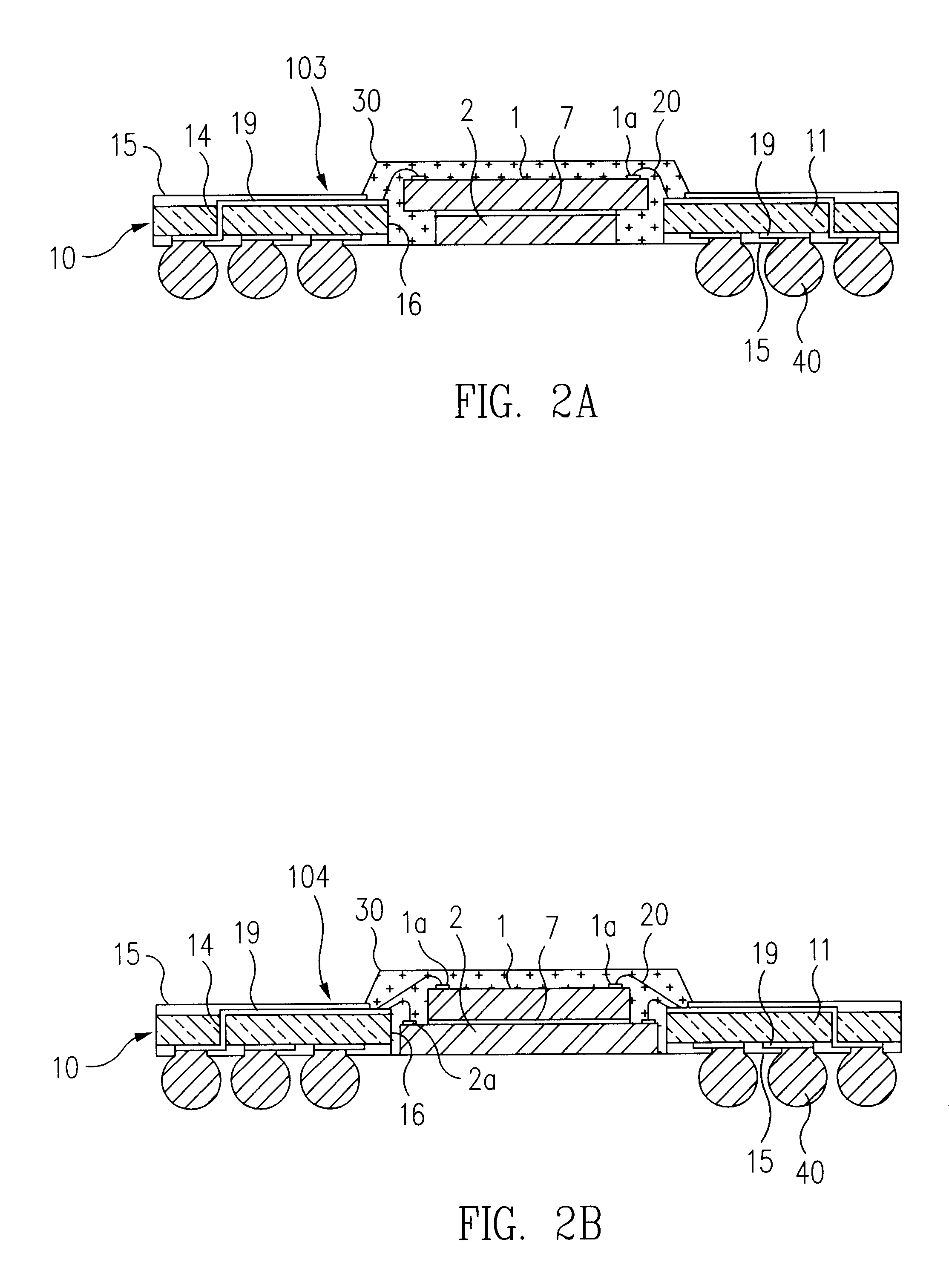
FIGS. 2A, 2B and 2C are cross sections showing semiconductor packages 103, 104 and 105 in accordance with the present invention.

The semiconductor packages 103, 104 and 105 of the second embodiment are similar to the semiconductor packages 101 and 102 of the first embodiment. The difference between them is described as follows.

In the drawings, reference numeral 1 designates a first semiconductor chip 1 on the lower surface of which input / output pads (not shown) are formed. A second semiconductor 2 is bonded on the surface, on which input / output pads (not shown) are formed, by means of a bonding layer 7. Input / output pads 2A are formed on the lower surface of the second semiconductor 2, also. The lower surface of the second semiconductor chip 2 is exposed out of an encapsulation 30 to improve the performance of heat dissipation.

A circuit board 10 is disposed around the first semiconductor chip 1. A predetermined-sized opening 16 is formed in the center portion of the circuit board 10,...

third embodiment

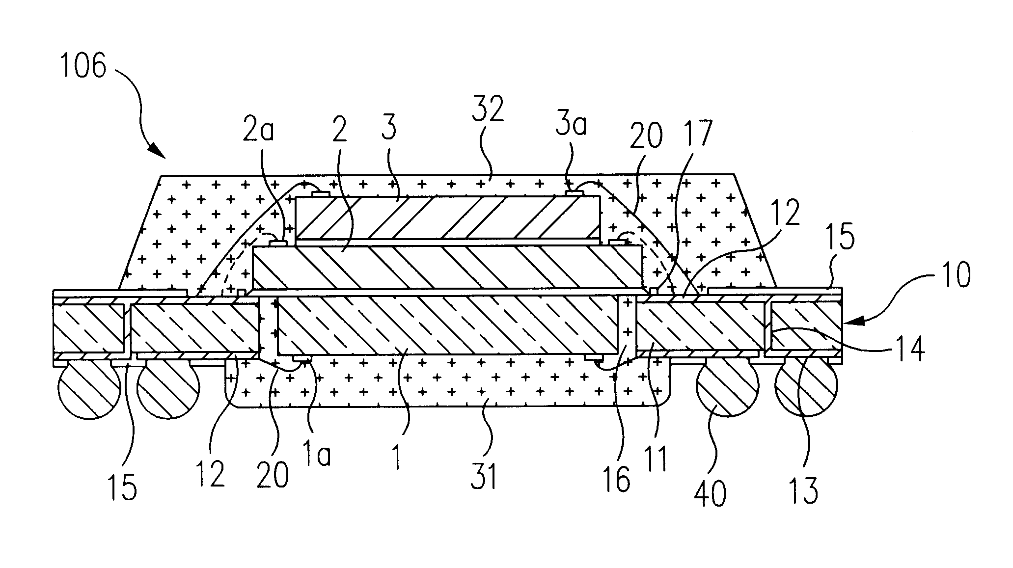
FIGS. 3A to 3C are cross sections showing semiconductor packages 106, 107 and 108 in accordance with the present invention.

As shown in FIG. 3A, reference numeral 10 designates a circuit board 10 for transmitting signals between a semiconductor chip and a motherboard. The circuit board 10 includes a resin layer 11 having an opening 16 at its center portion. Circuit patterns are formed on the upper and lower surfaces of the resin layer 11. In detail, the upper circuit pattern having bond fingers 12 is formed on the upper surface of the resin layer 11, while the lower circuit pattern having bond fingers and ball lands is formed on the lower surface of the resin layer 11. The circuit patterns formed on the upper and lower surfaces of the resin layer 11 are connected to each other through conductive via holes 14. The resin layer 11 is coated with cover coats 15 of a predetermined thickness at its upper and lower surfaces, with the bond fingers 12 and the ball lands 13 being exposed to th...


PUM


Abstract

A semiconductor package and method for fabricating the same is disclosed. In one embodiment, the semiconductor package includes a circuit board, at least two semiconductor chips, electric connection means, an encapsulant, and a plurality of conductive balls. The circuit board has a resin layer and a circuit pattern. The resin layer is provided with an opening at its center portion. The circuit pattern is formed on at least one of upper and lower surfaces of the resin layer and includes one or more bond fingers and ball lands exposed to the outside. The semiconductor chips have a plurality of input / output pads on an active surface thereof. The semiconductor chips are stacked at a position of the opening of the circuit board, with at least one of the chips being within the opening. Alternatively, both chips are in the opening. The electric connection means connects the input / output pads of the semiconductor chips to the bond fingers of the circuit board. The encapsulant surrounds the semiconductor chips so as to protect the chips from the external environment. The conductive balls are fusion-bonded on the ball lands of the circuit board.

Description

1. Field of the InventionThe present invention relates, in general, to a semiconductor package and method for fabricating the same and, more particularly, to a semiconductor package and method for fabricating the same that allows a plurality of semiconductor chips to be fixedly stacked in a single, thin package.2. Description of the Prior ArtCurrently, there is a tendency in which a plurality of semiconductor chips are packaged and mounted on the motherboard of an electronic device such as a PCS phone, a cellular phone or a notebook to perform various functions within a minimum time, and semiconductor packages in which semiconductor chips are packaged and the electronic devices on which the semiconductor packages are mounted are miniaturized. In the meantime, in order to allow a semiconductor package to be thinned, there has been fabricated a semiconductor package in which an opening is formed in a circuit board and a semiconductor is disposed in the opening.With reference to FIG. 7...

Claims


Application Information

Patent Timeline
Patent Type & Authority Patents(United States)
IPC IPC(8): H01L25/065H01L23/02H01L23/12H01L23/13H01L23/31H01L23/498H01L25/07H01L25/10H01L25/18
CPCH01L23/13H01L23/3128H01L23/49816H01L24/97H01L25/0657H01L25/105H01L2224/32145H01L2224/48091H01L2224/48227H01L2224/49171H01L2224/73265H01L2224/97H01L2225/0651H01L2225/06513H01L2225/06555H01L2225/06586H01L2924/01004H01L2924/01013H01L2924/01029H01L2924/01057H01L2924/01079H01L2924/14H01L2924/1433H01L2924/15311H01L2924/1532H01L2924/15331H01L2924/18165H01L24/48H01L2924/01005H01L2924/01033H01L24/49H01L2225/06568H01L2224/45144H01L2224/45124H01L2225/1035H01L2225/1058H01L2224/32225H01L2924/15321H01L2924/07802H01L2924/00014H01L2924/00H01L2924/00012H01L2924/181H01L24/45H01L24/73H01L2224/26175H01L2224/05599
Inventor SHIN, WON SUNCHUN, DO SUNGLEE, SEON GOOSHIM, IL KWONDICAPRIO, VINCENT
Owner AMKOR TECH SINGAPORE HLDG PTE LTD
Why Eureka
Try Eureka